AD7568BP Analog Devices Inc, AD7568BP Datasheet - Page 9
AD7568BP
Manufacturer Part Number
AD7568BP
Description
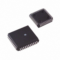
IC DAC 12BIT LC2MOS OCTAL 44PLCC
Manufacturer
Analog Devices Inc
Datasheet
1.AD7568BPZ-REEL.pdf
(12 pages)
Specifications of AD7568BP
Mounting Type
Surface Mount
Rohs Status
RoHS non-compliant
Settling Time
500ns
Number Of Bits
12
Data Interface
Serial
Number Of Converters
8
Voltage Supply Source
Single Supply
Power Dissipation (max)
17.5mW
Operating Temperature
-40°C ~ 85°C
Package / Case
44-PLCC
Resolution (bits)
12bit
No. Of Pins
44
Peak Reflow Compatible (260 C)
No
Update Rate
2MSPS
No. Of Bits
12 Bit
Leaded Process Compatible
No
No. Of Outputs
8
Resolution
12-Bit
Lead Free Status / RoHS Status
Contains lead / RoHS non-compliant
Available stocks
Company
Part Number
Manufacturer
Quantity
Price

Company:
Part Number:
AD7568BPZ
Manufacturer:
Analog Devices Inc
Quantity:
135
Company:
Part Number:
AD7568BPZ
Manufacturer:
Analog Devices Inc
Quantity:
10 000
Part Number:
AD7568BPZ
Manufacturer:
ADI/亚德诺
Quantity:
20 000
Company:
Part Number:
AD7568BPZ-REEL
Manufacturer:
Analog Devices Inc
Quantity:
10 000


REV. B
Current Mode Circuit
In the current mode circuit of Figure 17, I
I
operate correctly, the DAC ladder termination resistor must be
connected internally to I
The output voltage is given by:
As D varies from 0 to 4095/4096, the output voltage varies from
V
impedance source capable of sinking and sourcing all possible
variations in current at the I
problems.
Voltage Mode Circuit
Figure 18 shows DAC A of the AD7568 operating in the
voltage-switching mode. The reference voltage, V
the I
age is available at the V
positive reference voltage results in a positive output voltage
making single supply operation possible. The output from the
DAC is a voltage at a constant impedance (the DAC ladder re-
sistance). Thus, an op amp is necessary to buffer the output
voltage. The reference voltage input no longer sees a constant
input impedance, but one which varies with code. So, the volt-
age input should be driven from a low impedance source.
It is important to note that V
cause the switches in the DAC no longer have the same source-
drain voltage. As a result, their on-resistance differs and this
degrades the integral linearity of the DAC. Also, V
go negative by more than 0.3 volts or an internal diode will turn
on, causing possible damage to the device. This means that the
full-range multiplying capability of the DAC is lost.
OUT1
OUT
OUT1
, is biased positive by an amount V
= V
BIAS
pin, I
V
to V
OUT
OUT2
OUT
is connected to AGND and the output volt-
D
= 2 V
REF
OUT2
R
V
R
DAC
REF
FB
V
terminal. In this configuration, a
IN
OUT2
BIAS
A
. This is the case with the AD7568.
IN
V
is limited to low voltages be-
BIAS
– V
terminal without any
DAC A
(R1)
I
Figure 19. Programmable 2nd Order State Variable Filter
I
OUT1
IN
OUT2
V
. V
A
IN
A
BIAS
BIAS
OUT2
. For the circuit to
NOTES
1. A1, A2, A3, A4: 1/4 x AD713
2. DIGITAL INPUT CONNECTIONS ARE OMITTED.
3. C3 IS A COMPENSATION CAPACITOR TO ELIMINATE
I
I
should be a low
OUT1
OUT2
V
1/2 x AD7568
10k
Q AND GAIN VARIATIONS CAUSED BY AMPLIFIER GAIN
BANDWIDTH LIMITATIONS.
A1
, and hence
DAC B
BIAS
R6
(R2)
B
IN
B
IN
is applied to
R8 30k
R
must not
FB
B
V
A1
REF
B
V
REF
C3 10pF
R7 30k
–9–
HIGH
PASS
OUTPUT
C
DAC C
(R3)
APPLICATIONS
Programmable State Variable Filter
The AD7568 with its multiplying capability and fast settling
time is ideal for many types of signal conditioning applications.
The circuit of Figure 19 shows its use in a state variable filter
design. This type of filter has three outputs: low pass, high pass
and bandpass. The particular version shown in Figure 19 uses
one half of an AD7568 to control the critical parameters f
and A
DAC equivalent resistances as circuit elements. Thus, R1 in
Figure 19 is controlled by the 12-bit digital word loaded to
DAC A of the AD7568. This is also the case with R2, R3 and
R4. The fixed resistor R5 is the feedback resistor, R
where:
I
I
OUT2
OUT1
DAC Equivalent Resistance, R
R
N is the DAC Digital Code in Decimal (0 < N < 4096).
LADDER
C
C
0
. Instead of several fixed resistors, the circuit uses the
Figure 18. Single Supply Voltage Switching
Mode Operation
C1 1000pF
V
V
1) ONLY ONE DAC IS SHOWN FOR CLARITY.
2) DIGITAL INPUT CONNECTIONS ARE OMITTED.
3) C1 PHASE COMPENSATION (5–15pF) MAY BE
IN
NOTES
is the DAC ladder resistance.
REF
A2
DAC D
REQUIRED WHEN USING HIGH SPEED AMPLIFIER, A1.
(R4)
I
I
D
OUT1
OUT2
I
OUT2
A
A
D
I
C1 1000pF
OUT1
R
AD7568
DAC A
FB
A3
D
A
EQ
LOW
PASS
OUTPUT
BAND
PASS
OUTPUT
= (R
V
REF
R1
LADDER
A
A1
R2
AD7568
4096)/N
V
OUT
FB
B.
0
, Q
Related parts for AD7568BP
Image
Part Number
Description
Manufacturer
Datasheet
Request
R

Part Number:
Description:
±1.7g Dual-Axis IMEMS Accelerometer Evaluation Board
Manufacturer:
Analog Devices Inc
Datasheet:

Part Number:
Description:
Inertial Sensor Evaluation System
Manufacturer:
Analog Devices Inc
Datasheet:
Part Number:
Description:
Manufacturer:
Analog Devices Inc
Datasheet:
Part Number:
Description:
Manufacturer:
Analog Devices Inc
Datasheet:
Part Number:
Description:
Manufacturer:
Analog Devices Inc
Datasheet:
Part Number:
Description:
Manufacturer:
Analog Devices Inc
Datasheet:
Part Number:
Description:
Manufacturer:
Analog Devices Inc
Datasheet:
Part Number:
Description:
Manufacturer:
Analog Devices Inc
Datasheet:
Part Number:
Description:
Manufacturer:
Analog Devices Inc
Datasheet:
Part Number:
Description:
Manufacturer:
Analog Devices Inc
Datasheet:
Part Number:
Description:
Manufacturer:
Analog Devices Inc
Datasheet:
Part Number:
Description:
Manufacturer:
Analog Devices Inc
Datasheet:
Part Number:
Description:
Manufacturer:
Analog Devices Inc
Datasheet: