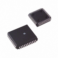
AD7568BP Analog Devices Inc, AD7568BP Datasheet - Page 7

AD7568BP
Manufacturer Part Number
AD7568BP
Description
IC DAC 12BIT LC2MOS OCTAL 44PLCC
Manufacturer
Analog Devices Inc
Datasheet
1.AD7568BPZ-REEL.pdf
(12 pages)
Specifications of AD7568BP
Mounting Type
Surface Mount
Rohs Status
RoHS non-compliant
Settling Time
500ns
Number Of Bits
12
Data Interface
Serial
Number Of Converters
8
Voltage Supply Source
Single Supply
Power Dissipation (max)
17.5mW
Operating Temperature
-40°C ~ 85°C
Package / Case
44-PLCC
Resolution (bits)
12bit
No. Of Pins
44
Peak Reflow Compatible (260 C)
No
Update Rate
2MSPS
No. Of Bits
12 Bit
Leaded Process Compatible
No
No. Of Outputs
8
Resolution
12-Bit
Lead Free Status / RoHS Status
Contains lead / RoHS non-compliant
Available stocks
Company
Part Number
Manufacturer
Quantity
Price
Company:
Part Number:
AD7568BPZ
Manufacturer:
Analog Devices Inc
Quantity:
135
Company:
Part Number:
AD7568BPZ
Manufacturer:
Analog Devices Inc
Quantity:
10 000
Part Number:
AD7568BPZ
Manufacturer:
ADI/亚德诺
Quantity:
20 000
Company:
Part Number:
AD7568BPZ-REEL
Manufacturer:
Analog Devices Inc
Quantity:
10 000
REV. B
GENERAL DESCRIPTION
D/A Section
The AD7568 contains eight 12-bit current-output D/A convert-
ers. A simplified circuit diagram for one of the D/A converters is
shown in Figure 13.
A segmented scheme is used whereby the 2 MSBs of the 12-bit
data word are decoded to drive the three switches A, B and C.
The remaining 10 bits of the data word drive the switches S0 to
S9 in a standard R–2R ladder configuration.
Each of the switches A to C steers 1/4 of the total reference cur-
rent with the remaining current passing through the R–2R
section.
Each DAC in the device has separate V
R
DACs in the same device to be configured differently.
When an output amplifier is connected in the standard configu-
ration of Figure 15, the output voltage is given by:
where D is the fractional representation of the digital word
loaded to the DAC. Thus, in the AD7568, D can be set from
0 to 4095/4096.
FB
C
pins. This makes the device extremely versatile and allows
V
2R
REF
Figure 12. Multiplying Frequency Response vs.
Digital Code
B
Figure 13. Simplified D/A Circuit Diagram
2R
–100
–10
–20
–30
–40
–50
–60
–70
–80
–90
A
0
10
3
2R
DAC LOADED WITH ALL 1s
V
T = +25 C
V
OP AMP = AD713
A
DD
IN
R
SHOWN FOR ALL 1s ON DAC
= 20V pk-pk
S9
= +5V
V
10
OUT
4
2R
DAC LOADED WITH ALL 0s
R
= –D
S8
10
5
2R
•
V
REF
REF
R
2R
10
S9
6
, I
OUT1
10
2R
, I
7
OUT2
R/2
and
R
I
I
OUT2
OUT1
FB
–7–
Interface Section
The AD7568 is a serial input device. Three lines control the se-
rial interface, FSIN, CLKIN and SDIN. The timing diagram is
shown in Figure 1.
When the FSIN input goes low, data appearing on the SDIN
line is clocked into the input shift register on each falling edge of
CLKIN. When sixteen bits have been received, the register
loading is automatically disabled until the next falling edge of
FSIN detected. Also, the received data is clocked out on the
next rising edge of CLKIN and appears on the SDOUT pin.
This feature allows several devices to be connected together in a
daisy chain fashion.
When the sixteen bits have been received in the input shift regis-
ter, DB3 (A0) is checked to see if it corresponds to the state of
pin A0. If it does, then the word is accepted. Otherwise, it is dis-
regarded. This allows the user to address one of two AD7568s
in a very simple fashion. DB0 to DB2 of the 16-bit word deter-
mine which of the eight DAC input latches is to be loaded.
When the LDAC line goes low, all eight DAC latches in the de-
vice are simultaneously loaded with the contents of their respec-
tive input latches, and the outputs change accordingly.
Bringing the CLR line low resets the DAC latches to all 0s. The
input latches are not affected, so that the user can revert to the
previous analog output if desired.
CLKIN
SDIN
FSIN
Figure 14. Input Logic
16-BIT INPUT SHIFT REGISTER
AD7568
SDOUT


