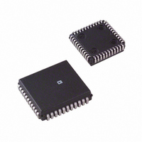
AD7568BP Analog Devices Inc, AD7568BP Datasheet - Page 5

AD7568BP
Manufacturer Part Number
AD7568BP
Description
IC DAC 12BIT LC2MOS OCTAL 44PLCC
Manufacturer
Analog Devices Inc
Datasheet
1.AD7568BPZ-REEL.pdf
(12 pages)
Specifications of AD7568BP
Mounting Type
Surface Mount
Rohs Status
RoHS non-compliant
Settling Time
500ns
Number Of Bits
12
Data Interface
Serial
Number Of Converters
8
Voltage Supply Source
Single Supply
Power Dissipation (max)
17.5mW
Operating Temperature
-40°C ~ 85°C
Package / Case
44-PLCC
Resolution (bits)
12bit
No. Of Pins
44
Peak Reflow Compatible (260 C)
No
Update Rate
2MSPS
No. Of Bits
12 Bit
Leaded Process Compatible
No
No. Of Outputs
8
Resolution
12-Bit
Lead Free Status / RoHS Status
Contains lead / RoHS non-compliant
Available stocks
Company
Part Number
Manufacturer
Quantity
Price
Company:
Part Number:
AD7568BPZ
Manufacturer:
Analog Devices Inc
Quantity:
135
Company:
Part Number:
AD7568BPZ
Manufacturer:
Analog Devices Inc
Quantity:
10 000
Part Number:
AD7568BPZ
Manufacturer:
ADI/亚德诺
Quantity:
20 000
Company:
Part Number:
AD7568BPZ-REEL
Manufacturer:
Analog Devices Inc
Quantity:
10 000
REV. B
TERMINOLOGY
Relative Accuracy
Relative Accuracy or endpoint linearity is a measure of the
maximum deviation from a straight line passing through the
endpoints of the DAC transfer function. It is measured after
adjusting for zero error and full-scale error and is normally ex-
pressed in Least Significant Bits or as a percentage or full-scale
reading.
Differential Nonlinearity
Differential nonlinearity is the difference between the measured
change and the ideal 1 LSB change between any two adjacent
codes. A specified differential nonlinearity of 1 LSB maximum
ensures monotonicity.
Gain Error
Gain Error is a measure of the output error between an ideal
DAC and the actual device output. It is measured with all 1s in
the DAC after offset error has been adjusted out and is
expressed in Least Significant Bits. Gain error is adjustable to
zero with an external potentiometer.
Output Leakage Current
Output leakage current is current which flows in the DAC lad-
der switches when these are turned off. For the I
it can be measured by loading all 0s to the DAC and measuring
the I
when the DAC is loaded with all 1s. This is a combination of
the switch leakage current and the ladder termination resistor
current. The I
I
Output Capacitance
This is the capacitance from the I
DB11 DB10 DB9
OUT1
DB15
OUT1
.
current. Minimum current will flow in the I
OUT2
leakage current is typically equal to that in
DB8
OUT1
DB7
pin to AGND.
DS2
0
0
0
0
1
1
1
1
DB6
Table I. AD7568 Loading Sequence
OUT1
DS1
0
0
1
1
0
0
1
1
DB5
OUT2
terminal,
Table II. DAC Selection
line
DB4
DS0
0
1
0
1
0
1
0
1
–5–
DB3
Output Voltage Settling Time
This is the amount of time it takes for the output to settle to a
specified level for a full-scale input change. For the AD7568, it
is specified with the AD843 as the output op amp.
Digital to Analog Glitch Impulse
This is the amount of charge injected into the analog output
when the inputs change state. It is normally specified as the area
of the glitch in either pA-secs or nV-secs, depending upon
whether the glitch is measured as a current or voltage signal. It
is measured with the reference input connected to AGND and
the digital inputs toggled between all 1s and all 0s.
AC Feedthrough Error
This is the error due to capacitive feedthrough from the DAC
reference input to the DAC I
loaded in the DAC.
Channel-to-Channel Isolation
Channel-to-channel isolation refers to the proportion of input
signal from one DAC’s reference input which appears at the
output of any other DAC in the device and is expressed in dBs.
Digital Crosstalk
The glitch impulse transferred to the output of one converter
due to a change in digital input code to the other converter is
defined as the Digital Crosstalk and is specified in nV-secs.
Digital Feedthrough
When the device is not selected, high frequency logic activity on
the device digital inputs is capacitively coupled through the de-
vice to show up as noise on the I
the op amp output. This noise is digital feedthrough.
Function
DAC A Selected
DAC B Selected
DAC C Selected
DAC D Selected
DAC E Sclected
DAC F Selected
DAC G Sclected
DAC H Selected
DB2
DB1
DB0
OUT
OUT
terminal, when all 0s are
A0
pin and subsequently on
DS2
AD7568
DS1
DB0
DS0


