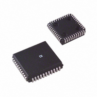
AD7568BP Analog Devices Inc, AD7568BP Datasheet - Page 2

AD7568BP
Manufacturer Part Number
AD7568BP
Description
IC DAC 12BIT LC2MOS OCTAL 44PLCC
Manufacturer
Analog Devices Inc
Datasheet
1.AD7568BPZ-REEL.pdf
(12 pages)
Specifications of AD7568BP
Mounting Type
Surface Mount
Rohs Status
RoHS non-compliant
Settling Time
500ns
Number Of Bits
12
Data Interface
Serial
Number Of Converters
8
Voltage Supply Source
Single Supply
Power Dissipation (max)
17.5mW
Operating Temperature
-40°C ~ 85°C
Package / Case
44-PLCC
Resolution (bits)
12bit
No. Of Pins
44
Peak Reflow Compatible (260 C)
No
Update Rate
2MSPS
No. Of Bits
12 Bit
Leaded Process Compatible
No
No. Of Outputs
8
Resolution
12-Bit
Lead Free Status / RoHS Status
Contains lead / RoHS non-compliant
Available stocks
Company
Part Number
Manufacturer
Quantity
Price
Company:
Part Number:
AD7568BPZ
Manufacturer:
Analog Devices Inc
Quantity:
135
Company:
Part Number:
AD7568BPZ
Manufacturer:
Analog Devices Inc
Quantity:
10 000
Part Number:
AD7568BPZ
Manufacturer:
ADI/亚德诺
Quantity:
20 000
Company:
Part Number:
AD7568BPZ-REEL
Manufacturer:
Analog Devices Inc
Quantity:
10 000
Parameter
ACCURACY
REFERENCE INPUT
DIGITAL INPUTS
POWER REQUIREMENTS
AC PERFORMANCE CHARACTERISTICS
Parameter
DYNAMIC PERFORMANCE
NOTES
1
2
Specifications subject to change without notice.
AD7568–SPECIFICATIONS
Temperature range as follows: B Version: –40 C to +85 C.
All specifications also apply for V
Resolution
Relative Accuracy
Differential Nonlinearity
Gain Error
Gain Temperature Coefficient
Output Leakage Current
Input Resistance
Ladder Resistance Mismatch
V
V
I
C
V
Power Supply Sensitivity
I
Output Voltage Settling Time
Digital to Analog Glitch Impulse
Multiplying Feedthrough Error
Output Capacitance
Channel-to-Channel Isolation
Digital Crosstalk
Digital Feedthrough
Total Harmonic Distortion
Output Noise Spectral Density
INH
DD
INH
INL
DD
IN
+25 C
T
I
@ 1 kHz
OUT1
, Input Capacitance
Gain/ V
MIN
, Input Current
, Input Low Voltage
@ +25 C
T
, Input High Voltage
Range
MIN
to T
to T
DD
MAX
MAX
REF
= +10 V, except relative accuracy which degrades to 1 LSB.
AD7568B
12
2
5
10
200
5
9
2
2.4
0.8
10
4.75/5.25
–75
300
3.5
AD7568B
500
40
–66
60
30
–76
40
40
–83
20
0.5
0.9
4
5
1
2
2
1
(V
unless otherwise noted)
V min/V max
ns typ
Units
Bits
LSB max
LSB max
LSBs max
LSBs max
ppm FSR/ C typ
ppm FSR/ C max
nA max
nA max
k min
k max
% max
V min
V max
pF max
dB typ
mA max
Units
nV–s typ
dB max
pF max
pF max
dB typ
nV–s typ
nV–s typ
dB typ
nV/ Hz
DD
A max
A max
(These characteristics are included for Design Guidance and are not subject
to test. DAC output op amp is AD843.)
= +4.75 V to +5.25 V; I
–2–
Test Conditions/Comments
1 LSB = V
All Grades Guaranteed Monotonic over Temperature
See Terminology Section
Typical Input Resistance = 7 k
Typically 0.6%
V
V
Test Conditions/Comments
To 0.01% of Full-Scale Range. DAC Latch Alternately
Loaded with All 0s and All 1s.
Measured with V
Loaded with All 0s and All 1s.
V
Loaded with All 0s.
All 1s Loaded to DAC.
All 0s Loaded to DAC.
Feedthrough from Any One Reference to the Others
with 20 V pk-pk, 10 kHz Sine Wave Applied.
Effect of all 0s to all 1s Code Transition on
Nonselected DACs.
Feedthrough to Any DAC Output with FSIN High
and Square Wave Applied to SDIN and SCLK.
V
All 1s Loaded to the DAC. V
Amp is AD OP07.
INH
INH
REF
REF
OUT1
= 4.0 V min, V
= 2.4 V min, V
= 20 V pk-pk, 10 kHz Sine Wave. DAC Latch
= 6 V rms, 1 kHz Sine Wave.
= I
OUT2
REF
= O V; V
/2
12
REF
= 1.22 mV when V
REF
INL
INL
= 0 V. DAC Register Alternately
= +5 V; T
= 0.4 V max
= 0.8 V max
REF
A
= 0 V. Output Op
= T
MIN
REF
to T
= 5 V
MAX
,
REV. B


