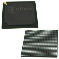
LFE3-150EA-8FN1156C Lattice, LFE3-150EA-8FN1156C Datasheet - Page 5

LFE3-150EA-8FN1156C
Manufacturer Part Number
LFE3-150EA-8FN1156C
Description
IC FPGA 149K LUTS 586I/O FN1156
Manufacturer
Lattice
Series
ECP3r
Datasheets
1.LFE3-150EA-7FN672C.pdf
(136 pages)
2.LFE3-35EA-8FN672I.pdf
(4 pages)
3.LFE3-35EA-8FN672I.pdf
(21 pages)
Specifications of LFE3-150EA-8FN1156C
Number Of Logic Elements/cells
149000
Number Of Labs/clbs
18625
Total Ram Bits
7014400
Number Of I /o
586
Number Of Gates
-
Voltage - Supply
1.14 V ~ 1.26 V
Mounting Type
Surface Mount
Operating Temperature
0°C ~ 85°C
Package / Case
1156-BBGA
Lead Free Status / Rohs Status
Lead free / RoHS Compliant
Available stocks
Company
Part Number
Manufacturer
Quantity
Price
Company:
Part Number:
LFE3-150EA-8FN1156C
Manufacturer:
Transcend
Quantity:
1 000
Part Number:
LFE3-150EA-8FN1156C
Manufacturer:
LATTICE
Quantity:
20 000
Company:
Part Number:
LFE3-150EA-8FN1156CTW
Manufacturer:
Lattice Semiconductor Corporation
Quantity:
10 000
Lattice Semiconductor
Figure 2-1. Simplified Block Diagram, LatticeECP3-35 Device (Top Level)
PFU Blocks
The core of the LatticeECP3 device consists of PFU blocks, which are provided in two forms, the PFU and PFF.
The PFUs can be programmed to perform Logic, Arithmetic, Distributed RAM and Distributed ROM functions. PFF
blocks can be programmed to perform Logic, Arithmetic and ROM functions. Except where necessary, the remain-
der of this data sheet will use the term PFU to refer to both PFU and PFF blocks.
Each PFU block consists of four interconnected slices numbered 0-3 as shown in Figure 2-2. Each slice contains
two LUTs. All the interconnections to and from PFU blocks are from routing. There are 50 inputs and 23 outputs
associated with each PFU block.
JTAG
Enhanced DSP
Slices: Multiply,
Accumulate and ALU
sysCLOCK
PLLs & DLLs:
Frequency Synthesis
and Clock Alignment
sysMEM Block
RAM: 18Kbit
Programmable
Function Units:
Up to 149K LUTs
Note: There is no Bank 4 or Bank 5 in LatticeECP3 devices.
sysIO
Bank
7
sysIO Bank 6
Bank 0
sysIO
SERDES/PCS
CH 3
SERDES/PCS
CH 2
2-2
SERDES/PCS
CH 1
SERDES/PCS
Bank 1
sysIO
CH 0
LatticeECP3 Family Data Sheet
3.2Gbps SERDES
sysIO Bank 3
sysIO
Bank
2
Configuration Logic:
Dual-boot, Encryption
and Transparent Updates
On-chip Oscillator
Pre-engineered Source
Synchronous Support:
DDR3 - 800Mbps
Generic - Up to 1Gbps
Flexible sysIO:
LVCMOS, HSTL,
SSTL, LVDS
Up to 486 I/Os
Flexible Routing:
Optimized for speed
and routability
Architecture


