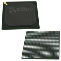
LFE3-150EA-8FN1156C Lattice, LFE3-150EA-8FN1156C Datasheet - Page 55

LFE3-150EA-8FN1156C
Manufacturer Part Number
LFE3-150EA-8FN1156C
Description
IC FPGA 149K LUTS 586I/O FN1156
Manufacturer
Lattice
Series
ECP3r
Datasheets
1.LFE3-150EA-7FN672C.pdf
(136 pages)
2.LFE3-35EA-8FN672I.pdf
(4 pages)
3.LFE3-35EA-8FN672I.pdf
(21 pages)
Specifications of LFE3-150EA-8FN1156C
Number Of Logic Elements/cells
149000
Number Of Labs/clbs
18625
Total Ram Bits
7014400
Number Of I /o
586
Number Of Gates
-
Voltage - Supply
1.14 V ~ 1.26 V
Mounting Type
Surface Mount
Operating Temperature
0°C ~ 85°C
Package / Case
1156-BBGA
Lead Free Status / Rohs Status
Lead free / RoHS Compliant
Available stocks
Company
Part Number
Manufacturer
Quantity
Price
Company:
Part Number:
LFE3-150EA-8FN1156C
Manufacturer:
Transcend
Quantity:
1 000
Part Number:
LFE3-150EA-8FN1156C
Manufacturer:
LATTICE
Quantity:
20 000
Company:
Part Number:
LFE3-150EA-8FN1156CTW
Manufacturer:
Lattice Semiconductor Corporation
Quantity:
10 000
Lattice Semiconductor
Hot Socketing Specifications
Hot Socketing Requirements
ESD Performance
IDK_HS
IDK
1. V
2. I
3. LVCMOS and LVTTL only.
4. Applicable to general purpose I/O pins located on the top and bottom sides of the device.
5. Applicable to general purpose I/O pins located on the left and right sides of the device.
Input current per SERDES I/O pin when device is powered down and inputs
driven.
1. Assumes the device is powered down, all supplies grounded, both P and N inputs driven by CML driver with maximum allowed VCCOB
2. Each P and N input must have less than the specified maximum input current. For a 16-channel device, the total input current would be
Symbol
(1.575V), 8b10b data, internal AC coupling.
8mA*16 channels *2 input pins per channel = 256mA
DK
5
CC
is additive to I
, V
All pins
All pins except high-speed serial and XRES
High-speed serial inputs
1. The XRES pin on the TW device passes CDM testing at 250V.
4
CCAUX
Input or I/O Leakage Current
Input or I/O Leakage Current
and V
PU
CCIO
, I
PW
Parameter
should rise/fall monotonically.
Pin Group
or I
BH
.
Description
0 V
0 V
V
CCIO
1, 2
1, 2, 3
IN
IN
1
V
V
< V
Condition
IN
IH
CCIO
V
(Max.)
ESD Stress
CCIO
3-2
HBM
CDM
CDM
+ 0.5V
DC and Switching Characteristics
Min.
Min.
—
—
—
—
LatticeECP3 Family Data Sheet
1000
Min.
500
400
Typ.
Typ.
18
—
—
—
Max.
Max.
+/-1
+/-1
Units
—
8
V
V
V
Units
Units
mA
mA
mA
mA


