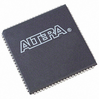
EPM9320LC84-15 Altera, EPM9320LC84-15 Datasheet - Page 18

EPM9320LC84-15
Manufacturer Part Number
EPM9320LC84-15
Description
IC MAX 9000 CPLD 320 84-PLCC
Manufacturer
Altera
Series
MAX® 9000r
Datasheet
1.EPM9320LC84-15.pdf
(46 pages)
Specifications of EPM9320LC84-15
Programmable Type
In System Programmable
Delay Time Tpd(1) Max
15.0ns
Voltage Supply - Internal
4.75 V ~ 5.25 V
Number Of Logic Elements/blocks
20
Number Of Macrocells
320
Number Of Gates
6000
Number Of I /o
60
Operating Temperature
0°C ~ 70°C
Mounting Type
Surface Mount
Package / Case
84-PLCC
Voltage
3.3V/5V
Memory Type
EEPROM
Number Of Logic Elements/cells
20
Lead Free Status / RoHS Status
Contains lead / RoHS non-compliant
Features
-
Other names
544-2362-5
Available stocks
Company
Part Number
Manufacturer
Quantity
Price
Company:
Part Number:
EPM9320LC84-15
Manufacturer:
ALTERA
Quantity:
1 560
Company:
Part Number:
EPM9320LC84-15
Manufacturer:
ALTERA20
Quantity:
51
Company:
Part Number:
EPM9320LC84-15N
Manufacturer:
ALTERA
Quantity:
4
MAX 9000 Programmable Logic Device Family Data Sheet
Output
Configuration
18
The output buffer in each IOC has an adjustable output slew rate that can
be configured for low-noise or high-speed performance. A slower slew
rate reduces board-level noise and adds a nominal timing delay to the
output buffer delay (t
speed-critical outputs in systems that are adequately protected against
noise. Designers can specify the slew rate on a pin-by-pin basis during
design entry or assign a default slew rate to all pins on a global basis. The
slew rate control affects both rising and falling edges of the output signals.
The MAX 9000 device architecture supports the MultiVolt I/O interface
feature, which allows MAX 9000 devices to interface with systems of
differing supply voltages. The 5.0-V devices in all packages can be set for
3.3-V or 5.0-V I/O pin operation. These devices have one set of V
for internal operation and input buffers (VCCINT), and another set for I/O
output drivers (VCCIO).
The VCCINT pins must always be connected to a 5.0-V power supply.
With a 5.0-V V
therefore compatible with 3.3-V and 5.0-V inputs.
Table 6. Peripheral Bus Sources
Peripheral Control
OE0/ENA0
OE1/ENA1
OE2/ENA2
OE3/ENA3
OE4/ENA4
OE5
OE6
OE7/CLR1
CLR0/ENA5
CLK0
CLK1
CLK2
CLK3
Signal
CCINT
Row C
Row B
Row A
Row B
Row A
Row D
Row C
Row B/GOE
Row A/GCLR Row A/GCLR Row A/GCLR Row A/GCLR
GCLK1
GCLK2
Row D
Row C
level, input voltages are at TTL levels and are
OD
EPM9320
EPM9320A
) parameter. The fast slew rate should be used for
Row E
Row E
Row E
Row B
Row A
Row D
Row C
Row B/GOE
GCLK1
GCLK2
Row D
Row C
EPM9400
Source
Row F
Row F
Row E
Row B
Row A
Row D
Row C
Row B/GOE
GCLK1
GCLK2
Row D
Row C
EPM9480
Altera Corporation
Row G
Row F
Row E
Row B
Row A
Row D
Row C
Row B/GOE
GCLK1
GCLK2
Row D
Row C
EPM9560
EPM9560A
CC
pins


