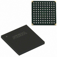
EPM240F100C5N Altera, EPM240F100C5N Datasheet - Page 22

EPM240F100C5N
Manufacturer Part Number
EPM240F100C5N
Description
IC MAX II CPLD 240 LE 100-FBGA
Manufacturer
Altera
Series
MAX® IIr
Specifications of EPM240F100C5N
Programmable Type
In System Programmable
Delay Time Tpd(1) Max
4.7ns
Voltage Supply - Internal
2.5V, 3.3V
Number Of Logic Elements/blocks
240
Number Of Macrocells
192
Number Of I /o
80
Operating Temperature
0°C ~ 85°C
Mounting Type
Surface Mount
Package / Case
100-FBGA
Voltage
2.5V, 3.3V
Memory Type
FLASH
Number Of Logic Elements/cells
240
Family Name
MAX II
# Macrocells
192
Frequency (max)
1.8797GHz
Propagation Delay Time
7.5ns
Number Of Logic Blocks/elements
24
# I/os (max)
80
Operating Supply Voltage (typ)
2.5/3.3V
In System Programmable
Yes
Operating Supply Voltage (min)
2.375V
Operating Supply Voltage (max)
3.6V
Operating Temp Range
0C to 85C
Operating Temperature Classification
Commercial
Mounting
Surface Mount
Pin Count
100
Package Type
FBGA
Lead Free Status / RoHS Status
Lead free / RoHS Compliant
Features
-
Lead Free Status / Rohs Status
Compliant
Other names
544-1709
Available stocks
Company
Part Number
Manufacturer
Quantity
Price
Company:
Part Number:
EPM240F100C5N
Manufacturer:
NSC
Quantity:
560
Company:
Part Number:
EPM240F100C5N
Manufacturer:
ALTERA
Quantity:
591
Part Number:
EPM240F100C5N
Manufacturer:
ALTERA/阿尔特拉
Quantity:
20 000
2–14
MAX II Device Handbook
functions from LE 1 to LE 10 in the same LAB. The register chain connection allows
the register output of one LE to connect directly to the register input of the next LE in
the LAB for fast shift registers. The Quartus II Compiler automatically takes
advantage of these resources to improve utilization and performance.
shows the LUT chain and register chain interconnects.
Figure 2–11. LUT Chain and Register Chain Interconnects
The C4 interconnects span four LABs up or down from a source LAB. Every LAB has
its own set of C4 interconnects to drive either up or down.
interconnect connections from an LAB in a column. The C4 interconnects can drive
and be driven by column and row IOEs. For LAB interconnection, a primary LAB or
its vertical LAB neighbor can drive a given C4 interconnect. C4 interconnects can
drive each other to extend their range as well as drive row interconnects for column-
to-column connections.
Interconnect
Adjacent LE
Routing to
LUT Chain
Local
Local Interconnect
Routing Among LEs
in the LAB
LE6
LE0
LE1
LE2
LE3
LE4
LE5
LE7
LE8
LE9
Register Chain
Routing to Adjacent
LE's Register Input
Figure 2–12
© October 2008 Altera Corporation
Chapter 2: MAX II Architecture
MultiTrack Interconnect
Figure 2–11
shows the C4


