CY7C371I-110JC Cypress Semiconductor Corp, CY7C371I-110JC Datasheet - Page 3
CY7C371I-110JC
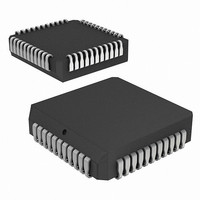
Manufacturer Part Number
CY7C371I-110JC
Description
IC CPLD 32 MACROCELL 44-PLCC
Manufacturer
Cypress Semiconductor Corp
Series
Ultralogic™r
Datasheet
1.CY7C371I-110JC.pdf
(12 pages)
Specifications of CY7C371I-110JC
Programmable Type
In-System Reprogrammable™ (ISR™) Flash
Delay Time Tpd(1) Max
10.0ns
Voltage Supply - Internal
4.75 V ~ 5.25 V
Number Of Logic Elements/blocks
2
Number Of Macrocells
32
Number Of I /o
32
Operating Temperature
0°C ~ 70°C
Mounting Type
Surface Mount
Package / Case
44-PLCC
Voltage
3.3V/5V
Memory Type
FLASH
Lead Free Status / RoHS Status
Contains lead / RoHS non-compliant
Features
-
Number Of Logic Elements/cells
-
Other names
428-1267
Available stocks
Company
Part Number
Manufacturer
Quantity
Price


set, V
another set, V
always be connected to a 5.0V power supply. However, the
V
supply, depending on the output requirements. When V
pins are connected to a 5.0V source, the I/O voltage levels are
compatible with 5.0V systems. When V
to a 3.3V source, the input voltage levels are compatible with
both 5.0V and 3.3V systems, while the output voltage levels
are compatible with 3.3V systems. There will be an additional
timing delay on all output buffers when operating in 3.3V I/O
mode. The added flexibility of 3.3V I/O capability is available
in commercial and industrial temperature ranges.
Bus Hold Capabilities on all I/Os and Dedicated Inputs
In addition to ISR capability, a new feature called bus-hold has
been added to all F
Bus-hold, which is an improved version of the popular internal
pull-up resistor, is a weak latch connected to the pin that does
not degrade the device’s performance. As a latch, bus-hold
recalls the last state of a pin when it is three-stated, thus re-
ducing system noise in bus-interface applications. Bus-hold
additionally allows unused device pins to remain unconnected
on the board, which is particularly useful during prototyping as
designers can route new signals to the device without cutting
trace connections to V
Operating Range
Document #: 38-03032 Rev. **
Commercial
Industrial
CCIO
Range
CCINT
pins may be connected to either a 3.3V or 5.0V power
, for internal operation and input buffers, and
CCIO
, for I/O output drivers. V
LASH
CC
Temperature
0 C to +70 C
40 C to +85 C
370i I/Os and dedicated input pins.
or GND.
Ambient
CCIO
pins are connected
CCINT
5V
5V
V
V
CCINT
pins must
CC
0.25V
0.5V
CCIO
3.3V
3.3V
5V
Design Tools
Development software for the CY7C371i is available from
Cypress’s Warp™, Warp Professional™, and Warp Enter-
prise™ software packages. Please refer to the data sheets on
these products for more details. Cypress also actively sup-
ports almost all third-party design tools. Please refer to
third-party tool support for further information.
Maximum Ratings
(Above which the useful life may be impaired. For user guide-
lines, not tested.)
Storage Temperature
Ambient Temperature with
Power Applied
Supply Voltage to Ground Potential
DC Voltage Applied to Outputs
in High Z State
DC Input Voltage
DC Program Voltage .................................................... 12.5V
Output Current into Outputs (LOW)............................. 16 mA
Static Discharge Voltage ........................................... >2001V
(per MIL-STD-883, Method 3015)
Latch-Up Current..................................................... >200 mA
5V
V
OR
OR
CCIO
0.25V
0.5V
0.3V
0.3V
65 C to +150 C
55 C to +125 C
CY7C371i
0.5V to +7.0V
0.5V to +7.0V
0.5V to +7.0V
Page 3 of 12
Related parts for CY7C371I-110JC
Image
Part Number
Description
Manufacturer
Datasheet
Request
R

Part Number:
Description:
Manufacturer:
Cypress Semiconductor Corp
Datasheet:

Part Number:
Description:
Manufacturer:
Cypress Semiconductor Corp
Datasheet:
Part Number:
Description:
Manufacturer:
Cypress Semiconductor Corp
Datasheet:
Part Number:
Description:
Manufacturer:
Cypress Semiconductor Corp
Datasheet:
Part Number:
Description:
Manufacturer:
Cypress Semiconductor Corp
Datasheet:
Part Number:
Description:
Manufacturer:
Cypress Semiconductor Corp
Datasheet:
Part Number:
Description:
Manufacturer:
Cypress Semiconductor Corp
Datasheet: