CY7C371I-110JC Cypress Semiconductor Corp, CY7C371I-110JC Datasheet - Page 6
CY7C371I-110JC
Manufacturer Part Number
CY7C371I-110JC
Description
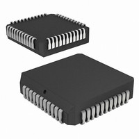
IC CPLD 32 MACROCELL 44-PLCC
Manufacturer
Cypress Semiconductor Corp
Series
Ultralogic™r
Datasheet
1.CY7C371I-110JC.pdf
(12 pages)
Specifications of CY7C371I-110JC
Programmable Type
In-System Reprogrammable™ (ISR™) Flash
Delay Time Tpd(1) Max
10.0ns
Voltage Supply - Internal
4.75 V ~ 5.25 V
Number Of Logic Elements/blocks
2
Number Of Macrocells
32
Number Of I /o
32
Operating Temperature
0°C ~ 70°C
Mounting Type
Surface Mount
Package / Case
44-PLCC
Voltage
3.3V/5V
Memory Type
FLASH
Lead Free Status / RoHS Status
Contains lead / RoHS non-compliant
Features
-
Number Of Logic Elements/cells
-
Other names
428-1267
Available stocks
Company
Part Number
Manufacturer
Quantity
Price


Switching Characteristics
Document #: 38-03032 Rev. **
Parameter
Combinatorial Mode Parameters
t
t
t
t
t
Input Registered/Latched Mode Parameters
t
t
t
t
t
t
Output Registered/Latched Mode Parameters
t
t
t
t
t
t
t
f
f
f
t
37x
Notes:
12. All AC parameters are measured with 16 outputs switching and 35-pF AC Test Load.
13. This specification is intended to guarantee interface compatibility of the other members of the CY7C370i family with the CY7C371i. This specification is met
PD
PDL
PDLL
EA
ER
WL
WH
IS
IH
ICO
ICOL
CO
S
H
CO2
SCS
SL
HL
MAX1
MAX2
MAX3
OH
-t
for the devices operating at the same ambient temperature and at the same power supply voltage.
IH
Input to Combinatorial Output
Input to Output Through Transparent Input or
Output Latch
Input to Output Through Transparent Input
and Output Latches
Input to Output Enable
Input to Output Disable
Clock or Latch Enable Input LOW Time
Clock or Latch Enable Input HIGH Time
Input Register or Latch Set-Up Time
Input Register or Latch Hold Time
Input Register Clock or Latch Enable to Com-
binatorial Output
Input Register Clock or Latch Enable to Out-
put Through Transparent Output Latch
Clock or Latch Enable to Output
Set-Up Time from Input to Clock or Latch
Enable
Register or Latch Data Hold Time
Output Clock or Latch Enable to Output Delay
(Through Memory Array)
Output Clock or Latch Enable to Output Clock
or Latch Enable (Through Memory Array)
Set-Up Time from Input Through Transparent
Latch to Output Register Clock or Latch En-
able
Hold Time for Input Through Transparent
Latch from Output Register Clock or Latch
Enable
Maximum Frequency with Internal Feedback
(Least of 1/t
Maximum Frequency Data Path in Output
Registered/Latched Mode (Lesser of 1/(t
t
Maximum Frequency with external feedback
(Lesser of 1/(t
Output Data Stable from Output clock Minus
Input Register Hold Time for 7C37x
WH
), 1/(t
S
+ t
SCS
[1]
H
CO
), or 1/t
, 1/(t
Description
[1]
+ t
[1]
S
S
Over the Operating Range
) and 1/(t
CO
+ t
[1]
)
H
[1]
[8]
), or 1/t
[1]
WL
[1]
CO
+ t
[8,13]
)
WH
[8]
[1]
))
[8]
WL
[8]
[8]
+
166.7
7C371i 143
[12]
Min.
143
2.5
2.5
91
2
2
5
0
7
9
0
0
Max.
13.5
11.5
8.5
13
13
12
14
12
6
153.8
7C371i 110
Min.
111
10
80
3
3
2
2
6
0
9
0
0
Max.
6.5
10
13
15
14
14
14
16
14
7C371iL 83
Min.
83.3
7C371i 83
100
12
12
50
4
4
3
3
8
0
0
0
Max.
12
18
20
19
19
19
21
19
8
7C371iL 66
Min.
66.6
83.3
41.6
7C371i 66
10
15
15
5
5
4
4
0
0
0
CY7C371i
Max.
Page 6 of 12
15
22
24
24
24
24
26
10
24
MHz
MHz
MHz
Unit
ns
ns
ns
ns
ns
ns
ns
ns
ns
ns
ns
ns
ns
ns
ns
ns
ns
ns
ns
Related parts for CY7C371I-110JC
Image
Part Number
Description
Manufacturer
Datasheet
Request
R

Part Number:
Description:
Manufacturer:
Cypress Semiconductor Corp
Datasheet:

Part Number:
Description:
Manufacturer:
Cypress Semiconductor Corp
Datasheet:
Part Number:
Description:
Manufacturer:
Cypress Semiconductor Corp
Datasheet:
Part Number:
Description:
Manufacturer:
Cypress Semiconductor Corp
Datasheet:
Part Number:
Description:
Manufacturer:
Cypress Semiconductor Corp
Datasheet:
Part Number:
Description:
Manufacturer:
Cypress Semiconductor Corp
Datasheet:
Part Number:
Description:
Manufacturer:
Cypress Semiconductor Corp
Datasheet: