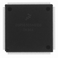
DSP56303AG100 Freescale Semiconductor, DSP56303AG100 Datasheet - Page 26

DSP56303AG100
Manufacturer Part Number
DSP56303AG100
Description
IC DSP 24BIT 100MHZ 144-LQFP
Manufacturer
Freescale Semiconductor
Series
DSP563xxr
Type
Fixed Pointr
Datasheet
1.DSP56303AG100.pdf
(108 pages)
Specifications of DSP56303AG100
Interface
Host Interface, SSI, SCI
Clock Rate
100MHz
Non-volatile Memory
ROM (576 B)
On-chip Ram
24kB
Voltage - I/o
3.30V
Voltage - Core
3.30V
Operating Temperature
-40°C ~ 100°C
Mounting Type
Surface Mount
Package / Case
144-LQFP
Package
144LQFP
Maximum Speed
100 MHz
Ram Size
24 KB
Device Million Instructions Per Second
100 MIPS
Lead Free Status / RoHS Status
Lead free / RoHS Compliant
Available stocks
Company
Part Number
Manufacturer
Quantity
Price
Company:
Part Number:
DSP56303AG100
Manufacturer:
Freescale Semiconductor
Quantity:
10 000
Company:
Part Number:
DSP56303AG100B1
Manufacturer:
Freescale Semiconductor
Quantity:
10 000
Company:
Part Number:
DSP56303AG100R2
Manufacturer:
Freescale Semiconductor
Quantity:
10 000
Specifications
2.5.4
2-6
No.
10
11
12
13
14
15
16
17
18
19
20
21
22
23
8
9
Delay from RESET assertion to all pins at reset value
Required RESET duration
•
•
•
•
•
•
Delay from asynchronous RESET deassertion to first external address
output (internal reset deassertion)
•
•
Synchronous reset set-up time from RESET deassertion to CLKOUT
Transition 1
•
•
Synchronous reset deasserted, delay time from the CLKOUT Transition
1 to the first external address output
•
•
Mode select setup time
Mode select hold time
Minimum edge-triggered interrupt request assertion width
Minimum edge-triggered interrupt request deassertion width
Delay from IRQA, IRQB, IRQC, IRQD, NMI assertion to external
memory access address out valid
•
•
Delay from IRQA, IRQB, IRQC, IRQD, NMI assertion to general-
purpose transfer output valid caused by first interrupt instruction
execution
Delay from address output valid caused by first interrupt instruction
execute to interrupt request deassertion for level sensitive fast
interrupts
Delay from RD assertion to interrupt request deassertion for level
sensitive fast interrupts
Delay from WR assertion to interrupt request deassertion for level
sensitive fast interrupts
•
•
•
•
Synchronous interrupt set-up time from IRQA, IRQB, IRQC, IRQD, NMI
assertion to the CLKOUT Transition 2
Synchronous interrupt delay time from the CLKOUT Transition 2 to the
first external address output valid caused by the first instruction fetch
after coming out of Wait Processing state
•
•
Power on, external clock generator, PLL disabled
Power on, external clock generator, PLL enabled
Power on, internal oscillator
During STOP, XTAL disabled (PCTL Bit 16 = 0)
During STOP, XTAL enabled (PCTL Bit 16 = 1)
During normal operation
Minimum
Maximum
Minimum
Maximum
Minimum
Maximum
Caused by first interrupt instruction fetch
Caused by first interrupt instruction execution
DRAM for all WS
SRAM WS = 1
SRAM WS = 2, 3
SRAM WS ≥ 4
Minimum
Maximum
Reset, Stop, Mode Select, and Interrupt Timing
1, 7, 8
1, 7, 8
1, 7, 8
Table 2-7.
4
Characteristics
5
Reset, Stop, Mode Select, and Interrupt Timing
DSP56303 Technical Data, Rev. 11
3
(WS + 3.75) × T
(WS + 3.25) × T
(WS + 3.5) × T
(WS + 3.5) × T
(WS + 2.5) × T
(WS + 3) × T
20.25 × T
24.75 × T
20.25 × T
3.25 × T
3.25 × T
4.25 × T
7.25 × T
8.25 × T
Expression
10 × T
75000 × ET
75000 × ET
1000 × ET
50 × ET
2.5 × T
2.5 × T
T
—
C
C
C
C
C
C
C
C
C
C
+ 5.0
C
+ 1.0
+ 2.0
+ 2.0
+ 1.0
+ 2.0
C
C
C
C
C
+ 1.0
+ 5.0
C
C
C
+ 10
– 10.94
C
– 10.94
– 10.94
– 10.94
C
C
– 10.94
– 10.94
6
Freescale Semiconductor
500.0
105.0
Min
10.0
0.75
0.75
25.0
25.0
34.5
33.5
30.0
44.5
74.5
83.5
5.9
0.0
6.6
6.6
5.9
—
—
—
—
—
—
—
—
—
—
—
100 MHz
Note 8
Note 8
Note 8
Note 8
Note 8
Note 8
212.5
203.5
252.5
Max
26.0
10.0
T
—
—
—
—
—
—
—
—
—
—
—
—
—
—
—
—
—
C
Unit
ms
ms
ns
ns
µs
ns
ns
ns
ns
ns
ns
ns
ns
ns
ns
ns
ns
ns
ns
ns
ns
ns
ns
ns
ns
ns
ns
ns
ns


