MSC8126TVT6400 Freescale Semiconductor, MSC8126TVT6400 Datasheet - Page 21
MSC8126TVT6400
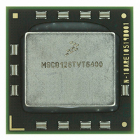
Manufacturer Part Number
MSC8126TVT6400
Description
IC DSP QUAD 16B 400MHZ 431FCPBGA
Manufacturer
Freescale Semiconductor
Series
MSC81xx StarCorer
Type
SC140 Corer
Datasheet
1.MSC8126TVT6400.pdf
(48 pages)
Specifications of MSC8126TVT6400
Interface
DSI, Ethernet, RS-232
Clock Rate
400MHz
Non-volatile Memory
External
On-chip Ram
1.436MB
Voltage - I/o
3.30V
Voltage - Core
1.20V
Operating Temperature
-40°C ~ 105°C
Mounting Type
Surface Mount
Package / Case
431-FCPBGA
Device Core Size
16b
Clock Freq (max)
400MHz
Mips
400
Device Input Clock Speed
400MHz
Operating Supply Voltage (typ)
1.1/1.1/1.2/1.2/3.3V
Operating Temp Range
-40C to 105C
Operating Temperature Classification
Industrial
Mounting
Surface Mount
Pin Count
431
Package Type
FCBGA
For Use With
MSC8126ADSE - KIT ADVANCED DEV SYSTEM 8126
Lead Free Status / RoHS Status
Lead free / RoHS Compliant
Available stocks
Company
Part Number
Manufacturer
Quantity
Price
Company:

Part Number:
MSC8126TVT6400
Manufacturer:
Freescale Semiconductor
Quantity:
135
Company:
Part Number:
MSC8126TVT6400
Manufacturer:
Freescale Semiconductor
Quantity:
10 000


2.5.4.3
Table 12 and Figure 9 describe the reset timing for a reset configuration write through the direct slave interface (DSI) or
through the system bus.
Freescale Semiconductor
Note:
No.
1
2
3
5
6
7
8
Required external PORESET duration minimum
•
•
•
Delay from deassertion of external PORESET to deassertion of internal
PORESET
•
Delay from de-assertion of internal PORESET to SPLL lock
•
•
•
Delay from SPLL to HRESET deassertion
•
Delay from SPLL lock to SRESET deassertion
•
Setup time from assertion of
CHIP_ID[0–3], BM[0–2], SWTE, and MODCK[1–2] before deassertion of
PORESET
Hold time from deassertion of PORESET to deassertion of
CNFGS, DSISYNC, DSI64, CHIP_ID[0–3], BM[0–2], SWTE, and
MODCK[1–2]
Timings are not tested, but are guaranteed by design.
Output (I/O)
CLKIN = 20 MHz
CLKIN = 133 MHz (400 MHz core)
CLKIN = 166 MHz (500 MHz core)
CLKIN = 20 MHz to 166 MHz
CLKIN = 20 MHz (RDF = 1)
CLKIN = 133 MHz (RDF = 2) (400 MHz core)
CLKIN = 166 MHz (RDF = 2) (500 MHz core)
REFCLK = 40 MHz to 166 MHz
REFCLK = 40 MHz to 166 MHz
Output (I/O)
PORESET
HRESET
SRESET
PORESET
Input
Table 12. Timing for a Reset Configuration Write through the DSI or System Bus
Internal
Reset Timing Tables
Figure 9. Timing Diagram for a Reset Configuration Write
MSC8126 Quad Digital Signal Processor Data Sheet, Rev. 15
1
Characteristics
RSTCONF
Reset configuration write
sequence during this
period.
RSTCONF, CNFGS, DSISYNC, DSI64
CHIP_ID[0–3], BM[0–2], SWTE, MODCK[1–2]
pins are sampled
Reset Configuration
, CNFGS, DSISYNC, DSI64,
Host programs
1 + 2
Word
2
RSTCONF
SPLL
locking period
MODCK[3–5]
,
3
clock-division factor)
6400/(CLKIN/RDF)
(PLL reference
Expression
512/REFCLK
515/REFCLK
1024/CLKIN
16/CLKIN
SPLL is locked
(no external indication)
Electrical Characteristics
5
6
6.17
3.08
3.10
Min
800
120
320
96
96
77
3
5
12.88
Max
51.2
12.8
800
320
96
77
—
—
—
—
Unit
ns
ns
ns
µs
µs
µs
µs
µs
µs
ns
ns
21
Related parts for MSC8126TVT6400
Image
Part Number
Description
Manufacturer
Datasheet
Request
R

Part Number:
Description:
Manufacturer:
Freescale Semiconductor, Inc
Datasheet:
Part Number:
Description:
Manufacturer:
Freescale Semiconductor, Inc
Datasheet:
Part Number:
Description:
Manufacturer:
Freescale Semiconductor, Inc
Datasheet:
Part Number:
Description:
Manufacturer:
Freescale Semiconductor, Inc
Datasheet:
Part Number:
Description:
Manufacturer:
Freescale Semiconductor, Inc
Datasheet:
Part Number:
Description:
Manufacturer:
Freescale Semiconductor, Inc
Datasheet:
Part Number:
Description:
Manufacturer:
Freescale Semiconductor, Inc
Datasheet:
Part Number:
Description:
Manufacturer:
Freescale Semiconductor, Inc
Datasheet:
Part Number:
Description:
Manufacturer:
Freescale Semiconductor, Inc
Datasheet:
Part Number:
Description:
Manufacturer:
Freescale Semiconductor, Inc
Datasheet:
Part Number:
Description:
Manufacturer:
Freescale Semiconductor, Inc
Datasheet:
Part Number:
Description:
Manufacturer:
Freescale Semiconductor, Inc
Datasheet:
Part Number:
Description:
Manufacturer:
Freescale Semiconductor, Inc
Datasheet:
Part Number:
Description:
Manufacturer:
Freescale Semiconductor, Inc
Datasheet:
Part Number:
Description:
Manufacturer:
Freescale Semiconductor, Inc
Datasheet: