MSC8126TVT6400 Freescale Semiconductor, MSC8126TVT6400 Datasheet - Page 42
MSC8126TVT6400
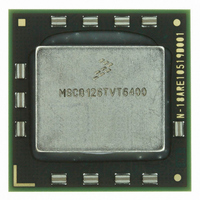
Manufacturer Part Number
MSC8126TVT6400
Description
IC DSP QUAD 16B 400MHZ 431FCPBGA
Manufacturer
Freescale Semiconductor
Series
MSC81xx StarCorer
Type
SC140 Corer
Datasheet
1.MSC8126TVT6400.pdf
(48 pages)
Specifications of MSC8126TVT6400
Interface
DSI, Ethernet, RS-232
Clock Rate
400MHz
Non-volatile Memory
External
On-chip Ram
1.436MB
Voltage - I/o
3.30V
Voltage - Core
1.20V
Operating Temperature
-40°C ~ 105°C
Mounting Type
Surface Mount
Package / Case
431-FCPBGA
Device Core Size
16b
Clock Freq (max)
400MHz
Mips
400
Device Input Clock Speed
400MHz
Operating Supply Voltage (typ)
1.1/1.1/1.2/1.2/3.3V
Operating Temp Range
-40C to 105C
Operating Temperature Classification
Industrial
Mounting
Surface Mount
Pin Count
431
Package Type
FCBGA
For Use With
MSC8126ADSE - KIT ADVANCED DEV SYSTEM 8126
Lead Free Status / RoHS Status
Lead free / RoHS Compliant
Available stocks
Company
Part Number
Manufacturer
Quantity
Price
Company:

Part Number:
MSC8126TVT6400
Manufacturer:
Freescale Semiconductor
Quantity:
135
Company:
Part Number:
MSC8126TVT6400
Manufacturer:
Freescale Semiconductor
Quantity:
10 000


Hardware Design Considerations
3.3
Unused output pins can be disconnected, and unused input pins should be connected to the non-active value, via resistors to
V
Note:
42
DDH
•
•
•
•
•
•
•
•
•
•
•
•
•
•
or
GND
If the DSI is unused (DDR[DSIDIS] is set),
disconnected.
When the DSI uses synchronous mode,
up or down, depending on design requirements.
HDST
DCR[DSRFA] bit is set.
When the DSI is in 64-bit data bus mode and DCR[BEM] is cleared, pull up
HDBE[1–3]
When the DSI is in 32-bit data bus mode and DCR[BEM] is cleared,
must be pulled up.
When the DSI is in asynchronous mode,
When the DSI uses sliding window address mode (DCR[SLDWA] = 1), the external HA[11–13] signals must be
connected (tied) to the correct voltage levels so that the host can perform the first access to the DCR. After reset, the
DSI expects full address mode (DCR[SLDWA] = 0). The DCR address in the DSI memory map is 0x1BE000, which
requires the following connections:
— HA11 must be pulled high (1)
— HA12 must be pulled high (1)
— HA13 must be pulled low (0)
The following signals must be pulled up:
In single-master mode (BCR[EBM] = 0) with internal arbitration (PPC_ACR[EARB] = 0):
—
—
—
—
If there is an external bus master (BCR[EBM] = 1):
—
—
In single-master mode,
modes, they must be pulled up.
The MSC8126 does not support DLL-enabled mode. For the following two clock schemes, ensure that the DLL is
disabled (that is, the DLLDIS bit in the Hard Reset Configuration Word is set).
If no system synchronization is required (for example, the design does not use SDRAM), you can use any of the
available clock modes.
In the
— Connect the oscillator output through a buffer to
— Connect
— Valid clock modes in this scheme are: 0, 7, 15, 19, 21, 23, 28, 29, 30, and 31.
In
connections:
— Connect the oscillator output through a buffer to
— Connect
CLKOUT
Connectivity Guidelines
BG
EXT_BG[2–3]
functionality. For any other functionality, connect the signal lines based on the multiplexed functionality.
BR
EXT_BR[2–3]
BR
EXT_BR[2–3]
functionality.
between the clock buffer to the MSC8126 and the SDRAM is equal (that is, has a skew less than 100 ps).
guidelines:
– The maximum delay between the slave and
, except for the following:
CLKIN
can be disconnected if the DSI is in big-endian mode, or if the DSI is in little-endian mode and the
,
,
must be pulled up.
DBG
BG
,
and
synchronization mode (for 1.2 V devices),
DBG
, and
the CLKIN
CLKOUT
synchronization mode, use the following connections:
HWBS[4–7]
, and
,
,
TS
must be pulled up if multiplexed to the system bus functionality.
EXT_BG[2–3]
EXT_DBG[2–3]
MSC8126 Quad Digital Signal Processor Data Sheet, Rev. 15
can be left unconnected.
TS
through a zero-delay buffer to the slave device (for example, SDRAM) using the following
ABB
buffer output to the slave device (for example, SDRAM) making sure that the delay path
must be pulled up.
/
and
HDBS[4–7]
DBB
, and
, and
can be selected as
EXT_DBG[2–3]
/
HTA
HWBE[4–7]
GBL
HBRST
HRESET
HCS
must be pulled up. In asynchronous mode,
can be left unconnected if they are multiplexed to the system bus
and
and
,
SRESET
CLKOUT
/
HDBE[4–7]
HCLKIN
CLKIN
CLKIN
HBCS
must be pulled up if multiplexed to the system bus
CLKOUT
IRQ
.
.
,
inputs and be connected to the non-active value. In other
must pulled up and all the rest of the DSI signals can be
ARTRY
must not exceed 0.7 ns.
should either be disconnected or pulled up.
/
PWE[4–7]
is the main clock to SDRAM. Use the following
HWBS[1–3]
,
TA
,
TEA
/
PSDDQM[4–7]
HWBS[1–3]
,
PSDVAL
/
HDBS[1–3]
HTA
/
, and
HDBS[1–3]
/
PBS[4–7]
Freescale Semiconductor
/
should be pulled either
HWBE[1–3]
AACK
.
/
.
HWBE[1–3]
/
HDBE[1–3]
/
Related parts for MSC8126TVT6400
Image
Part Number
Description
Manufacturer
Datasheet
Request
R

Part Number:
Description:
Manufacturer:
Freescale Semiconductor, Inc
Datasheet:
Part Number:
Description:
Manufacturer:
Freescale Semiconductor, Inc
Datasheet:
Part Number:
Description:
Manufacturer:
Freescale Semiconductor, Inc
Datasheet:
Part Number:
Description:
Manufacturer:
Freescale Semiconductor, Inc
Datasheet:
Part Number:
Description:
Manufacturer:
Freescale Semiconductor, Inc
Datasheet:
Part Number:
Description:
Manufacturer:
Freescale Semiconductor, Inc
Datasheet:
Part Number:
Description:
Manufacturer:
Freescale Semiconductor, Inc
Datasheet:
Part Number:
Description:
Manufacturer:
Freescale Semiconductor, Inc
Datasheet:
Part Number:
Description:
Manufacturer:
Freescale Semiconductor, Inc
Datasheet:
Part Number:
Description:
Manufacturer:
Freescale Semiconductor, Inc
Datasheet:
Part Number:
Description:
Manufacturer:
Freescale Semiconductor, Inc
Datasheet:
Part Number:
Description:
Manufacturer:
Freescale Semiconductor, Inc
Datasheet:
Part Number:
Description:
Manufacturer:
Freescale Semiconductor, Inc
Datasheet:
Part Number:
Description:
Manufacturer:
Freescale Semiconductor, Inc
Datasheet:
Part Number:
Description:
Manufacturer:
Freescale Semiconductor, Inc
Datasheet: