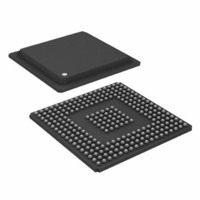
ADSP-BF535PKB-350 Analog Devices Inc, ADSP-BF535PKB-350 Datasheet - Page 30

ADSP-BF535PKB-350
Manufacturer Part Number
ADSP-BF535PKB-350
Description
IC DSP CONTROLLER 16BIT 260 BGA
Manufacturer
Analog Devices Inc
Series
Blackfin®r
Type
Fixed Pointr
Specifications of ADSP-BF535PKB-350
Rohs Status
RoHS non-compliant
Interface
PCI, SPI, SSP, UART, USB
Clock Rate
350MHz
Non-volatile Memory
External
On-chip Ram
308kB
Voltage - I/o
3.30V
Voltage - Core
1.60V
Operating Temperature
0°C ~ 70°C
Mounting Type
Surface Mount
Package / Case
260-BGA
Device Core Size
32b
Architecture
Modified Harvard
Format
Floating Point
Clock Freq (max)
350MHz
Device Input Clock Speed
350MHz
Program Memory Size
Not RequiredKB
Operating Temp Range
0C to 70C
Operating Temperature Classification
Commercial
Mounting
Surface Mount
Package Type
BGA
Lead Free Status / Rohs Status
Not Compliant
Available stocks
Company
Part Number
Manufacturer
Quantity
Price
Company:
Part Number:
ADSP-BF535PKB-350
Manufacturer:
Analog Devices Inc
Quantity:
10 000
Company:
Part Number:
ADSP-BF535PKB-350 1.3
Manufacturer:
ADI
Quantity:
246
ADSP-BF535
Serial Ports
Table 17
timing.
Table 17. Serial Ports—External Clock
1
Table 18. Serial Ports—Internal Clock
1
Table 19. Serial Ports—External or Internal Clock
1
Table 20. Serial Ports—External Clock
1
Table 21. Serial Ports—Internal Clock
1
Parameter
Timing Requirements
t
t
t
t
t
t
Parameter
Timing Requirements
t
t
t
t
Parameter
Switching Characteristics
t
t
Parameter
Switching Characteristics
t
t
t
t
Parameter
Switching Characteristics
t
t
t
t
t
Referenced to sample edge.
Referenced to sample edge.
Referenced to drive edge.
Referenced to drive edge.
Referenced to drive edge.
SFSE
HFSE
SDRE
HDRE
SCLKWE
SCLKE
SFSI
HFSI
SDRI
HDRI
DFSE
HOFSE
DFSE
HOFSE
DDTE
HDTE
DFSI
HOFSI
DDTI
HDTI
SCLKWI
through
Table 22
TFS/RFS Setup Before TCLK/RCLK
TFS/RFS Hold After TCLK/RCLK
Receive Data Setup Before RCLK
Receive Data Hold Before RCLK
TCLK/RCLK Width
TCLK/RCLK Period
TFS/RFS Setup Before TCLK/RCLK
TFS/RFS Hold After TCLK/RCLK
Receive Data Setup Before RCLK
Receive Data Hold Before RCLK
RFS Delay After RCLK (Internally Generated RFS)
RFS Hold After RCLK (Internally Generated RFS)
TFS Delay After TCLK (Internally Generated TFS)
TFS Hold After TCLK (Internally Generated TFS)
Transmit Data Delay After TCLK
Transmit Data Hold After TCLK
TFS Delay After TCLK (Internally Generated TFS)
TFS Hold After TCLK (Internally Generated TFS)
Transmit Data Delay After TCLK
Transmit Data Hold After TCLK
TCLK/RCLK Width
and
Figure 14
describe Serial Port
1
1
1
1
1
1
1
1
1
1
1
1
–30–
1
1
1
1
1
1
Min
3.0
3.0
3.0
3.0
(0.5 t
2 t
Min
7.0
2.0
7.0
4.0
Min
3.0
Min
3.0
3.0
Min
0.0
0.0
0.5 t
SCLK
SCLK
SCLKE
) – 1
Max
10.0
Max
10.0
10.0
Max
Max
6.0
8.0
Max
REV. A
Unit
ns
ns
Unit
ns
ns
ns
ns
Unit
ns
ns
ns
ns
Unit
ns
ns
ns
ns
ns
Unit
ns
ns
ns
ns
ns
ns


