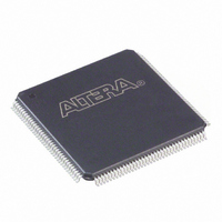
EPF6016TC144-3N Altera, EPF6016TC144-3N Datasheet - Page 5

EPF6016TC144-3N
Manufacturer Part Number
EPF6016TC144-3N
Description
IC FLEX 6000 FPGA 16K 144-TQFP
Manufacturer
Altera
Series
FLEX 6000r
Datasheet
1.EPF6010ATC100-3N.pdf
(52 pages)
Specifications of EPF6016TC144-3N
Number Of Logic Elements/cells
1320
Number Of Labs/clbs
132
Number Of I /o
117
Number Of Gates
16000
Voltage - Supply
4.75 V ~ 5.25 V
Mounting Type
Surface Mount
Operating Temperature
0°C ~ 85°C
Package / Case
144-TQFP, 144-VQFP
Family Name
FLEX 6000
Number Of Usable Gates
16000
Number Of Logic Blocks/elements
1320
# I/os (max)
117
Frequency (max)
125MHz
Process Technology
SRAM
Operating Supply Voltage (typ)
5V
Logic Cells
1320
Device System Gates
16000
Operating Supply Voltage (min)
4.75V
Operating Supply Voltage (max)
5.25V
Operating Temp Range
0C to 85C
Operating Temperature Classification
Commercial
Mounting
Surface Mount
Pin Count
144
Package Type
TQFP
Lead Free Status / RoHS Status
Lead free / RoHS Compliant
Total Ram Bits
-
Lead Free Status / Rohs Status
Compliant
Other names
544-1956
EPF6016TC144-3N
EPF6016TC144-3N
Available stocks
Company
Part Number
Manufacturer
Quantity
Price
Company:
Part Number:
EPF6016TC144-3N
Manufacturer:
ALTERA42
Quantity:
1 341
Part Number:
EPF6016TC144-3N
Manufacturer:
ALTERA/阿尔特拉
Quantity:
20 000
Functional
Description
Altera Corporation
The FLEX 6000 OptiFLEX architecture consists of logic elements (LEs).
Each LE includes a 4-input look-up table (LUT), which can implement any
4-input function, a register, and dedicated paths for carry and cascade
chain functions. Because each LE contains a register, a design can be easily
pipelined without consuming more LEs. The specified gate count for
FLEX 6000 devices includes all LUTs and registers.
LEs are combined into groups called logic array blocks (LABs); each LAB
contains 10 LEs. The Altera software automatically places related LEs into
the same LAB, minimizing the number of required interconnects. Each
LAB can implement a medium-sized block of logic, such as a counter or
multiplexer.
Signal interconnections within FLEX 6000 devices—and to and from
device pins—are provided via the routing structure of the FastTrack
Interconnect. The routing structure is a series of fast, continuous row and
column channels that run the entire length and width of the device. Any
LE or pin can feed or be fed by any other LE or pin via the FastTrack
Interconnect. See “FastTrack Interconnect” on
for more information.
Each I/O pin is fed by an I/O element (IOE) located at the end of each row
and column of the FastTrack Interconnect. Each IOE contains a
bidirectional I/O buffer. Each IOE is placed next to an LAB, where it can
be driven by the local interconnect of that LAB. This feature allows fast
clock-to-output times of less than 8 ns when a pin is driven by any of the
10 LEs in the adjacent LAB. Also, any LE can drive any pin via the row and
column interconnect. I/O pins can drive the LE registers via the row and
column interconnect, providing setup times as low as 2 ns and hold times
of 0 ns. IOEs provide a variety of features, such as JTAG BST support,
slew-rate control, and tri-state buffers.
Figure 1
Each group of ten LEs is combined into an LAB, and the LABs are
arranged into rows and columns. The LABs are interconnected by the
FastTrack Interconnect. IOEs are located at the end of each FastTrack
Interconnect row and column.
shows a block diagram of the FLEX 6000 OptiFLEX architecture.
FLEX 6000 Programmable Logic Device Family Data Sheet
page 17
of this data sheet
5


