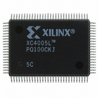
XC4005L-5PQ100C Xilinx Inc, XC4005L-5PQ100C Datasheet - Page 27

XC4005L-5PQ100C
Manufacturer Part Number
XC4005L-5PQ100C
Description
IC 3.3V FPGA 196 CLB'S 100-PQFP
Manufacturer
Xilinx Inc
Series
XC4000r
Datasheet
1.XC4005L-5PC84C.pdf
(175 pages)
Specifications of XC4005L-5PQ100C
Number Of Logic Elements/cells
466
Number Of Labs/clbs
196
Total Ram Bits
6272
Number Of I /o
77
Number Of Gates
5000
Voltage - Supply
3 V ~ 3.6 V
Mounting Type
Surface Mount
Operating Temperature
0°C ~ 85°C
Package / Case
100-BQFP
Lead Free Status / RoHS Status
Contains lead / RoHS non-compliant
Other names
122-1121
Available stocks
Company
Part Number
Manufacturer
Quantity
Price
Wide Edge Decoders
Dedicated decoder circuitry boosts the performance of
wide decoding functions. When the address or data field is
wider than the function generator inputs, FPGAs need
multi-level decoding and are thus slower than PALs.
XC4000-Series CLBs have nine inputs. Any decoder of up
to nine inputs is, therefore, compact and fast. However,
there is also a need for much wider decoders, especially for
address decoding in large microprocessor systems.
An XC4000-Series FPGA has four programmable decod-
ers located on each edge of the device. The inputs to each
decoder are any of the IOB I1 signals on that edge plus one
local interconnect per CLB row or column. Each row or col-
umn of CLBs provides up to three variables or their compli-
ments., as shown in
High output (resistor pull-up) when the AND condition of
the selected inputs, or their complements, is true. This is
analogous to a product term in typical PAL devices.
Each of these wired-AND gates is capable of accepting up
to 42 inputs on the XC4005E and 72 on the XC4013E.
There are up to 96 inputs for each decoder on the
XC4028EX and 132 on the XC4052EX. The decoders may
also be split in two when a larger number of narrower
decoders are required, for a maximum of 32 decoders per
device.
The decoder outputs can drive CLB inputs, so they can be
combined with other logic to form a PAL-like AND/OR struc-
ture. The decoder outputs can also be routed directly to the
chip outputs. For fastest speed, the output should be on
the same chip edge as the decoder. Very large PALs can
be emulated by ORing the decoder outputs in a CLB. This
decoding feature covers what has long been considered a
weakness of older FPGAs. Users often resorted to exter-
nal PALs for simple but fast decoding functions. Now, the
dedicated decoders in the XC4000-Series device can
implement these functions fast and efficiently.
To use the wide edge decoders, place one or more of the
WAND library symbols (WAND1, WAND4, WAND8,
WAND16). Attach a DECODE attribute or property to each
WAND symbol. Tie the outputs together and attach a PUL-
LUP symbol. Location attributes or properties such as L
(left edge) or TR (right half of top edge) should also be used
to ensure the correct placement of the decoder inputs.
September 18, 1996 (Version 1.04)
Figure
24. Each decoder generates a
On-Chip Oscillator
XC4000-Series devices include an internal oscillator. This
oscillator is used to clock the power-on time-out, for config-
uration memory clearing, and as the source of CCLK in
Master configuration modes. The oscillator runs at a nom-
inal 8 MHz frequency that varies with process, Vcc, and
temperature. The output frequency falls between 4 and 10
MHz. (The oscillator operates more slowly at lower volt-
ages. The output frequency may be reduced by as much
as 10% for low-voltage devices.)
The oscillator output is optionally available after configura-
tion. Any two of four resynchronized taps of a built-in
divider are also available. These taps are at the fourth,
ninth, fourteenth and nineteenth bits of the divider. There-
fore, if the primary oscillator output is running at the nomi-
nal 8 MHz, the user has access to an 8 MHz clock, plus any
two of 500 kHz, 16kHz, 490Hz and 15Hz (up to 10% lower
for low-voltage devices). These frequencies can vary by as
much as -50% or +25%.
These signals can be accessed by placing the OSC4
library element in a schematic or in HDL code (see
Figure
The oscillator is automatically disabled after configuration if
the OSC4 symbol is not used in the design.
Figure 24: XC4000-Series Edge Decoding Example
Figure 25: XC4000-Series Oscillator Symbol
25).
IOB
A
.I1
INTERCONNECT
OSC4
C
F500K
F16K
F490
F8M
F15
X6703
IOB
B
.I1
(
(A • B • C) .....
(A • B • C) .....
(A • B • C) .....
C) .....
X2627
4-31


