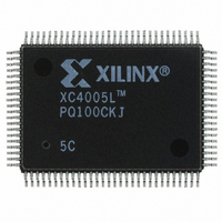
XC4005L-5PQ100C Xilinx Inc, XC4005L-5PQ100C Datasheet - Page 56

XC4005L-5PQ100C
Manufacturer Part Number
XC4005L-5PQ100C
Description
IC 3.3V FPGA 196 CLB'S 100-PQFP
Manufacturer
Xilinx Inc
Series
XC4000r
Datasheet
1.XC4005L-5PC84C.pdf
(175 pages)
Specifications of XC4005L-5PQ100C
Number Of Logic Elements/cells
466
Number Of Labs/clbs
196
Total Ram Bits
6272
Number Of I /o
77
Number Of Gates
5000
Voltage - Supply
3 V ~ 3.6 V
Mounting Type
Surface Mount
Operating Temperature
0°C ~ 85°C
Package / Case
100-BQFP
Lead Free Status / RoHS Status
Contains lead / RoHS non-compliant
Other names
122-1121
Available stocks
Company
Part Number
Manufacturer
Quantity
Price
XC4000 Series Field Programmable Gate Arrays
Configuration
The 0010 preamble code, included for all modes except
Express mode, indicates that the following 24 bits repre-
sent the length count. The length count is the total number
of configuration clocks needed to load the complete config-
uration data.
required to complete the configuration process, as dis-
cussed below.) After the preamble and the length count
have been passed through to all devices in the daisy chain,
DOUT is held High to prevent frame start bits from reaching
any daisy-chained devices. In Express mode, the length
count bits are ignored, and DOUT is held Low, to disable
the next device in the pseudo daisy chain.
A specific configuration bit, early in the first frame of a mas-
ter device, controls the configuration-clock rate and can
increase it by a factor of eight. Therefore, if a fast configu-
ration clock is selected by the bitstream, the slower clock
rate is used until this configuration bit is detected.
Each frame has a start field followed by the frame-configu-
ration data bits and a frame error field. If a frame data error
is detected, the FPGA halts loading, and signals the error
by pulling the open-drain INIT pin Low. After all configura-
tion frames have been loaded into an FPGA, DOUT again
follows the input data so that the remaining data is passed
on to the next device. In Express mode, when the first
device is fully programmed, DOUT goes High to enable the
next device in the chain.
Delaying Configuration After Power-Up
There are two methods of delaying configuration after
power-up: put a logic Low on the PROGRAM input, or pull
the bidirectional INIT pin Low, using an open-collector
(open-drain) driver. (See
A Low on the PROGRAM input is the more radical
approach, and is recommended when the power-supply
rise time is excessive or poorly defined. As long as PRO-
GRAM is Low, the FPGA keeps clearing its configuration
memory. When PROGRAM goes High, the configuration
memory is cleared one more time, followed by the begin-
ning of configuration, provided the INIT input is not exter-
nally held Low. Note that a Low on the PROGRAM input
automatically forces a Low on the INIT output. The
XC4000-Series PROGRAM pin has a permanent weak
pull-up.
Using an open-collector or open-drain driver to hold INIT
Low before the beginning of configuration causes the
FPGA to wait after completing the configuration memory
clear operation. When INIT is no longer held Low exter-
nally, the device determines its configuration mode by cap-
turing its mode pins, and is ready to start the configuration
process. A master device waits up to an additional 250 s
4-60
(Four additional configuration clocks are
Figure 48 on page
59.)
to make sure that any slaves in the optional daisy chain
have seen that INIT is High.
Start-Up
Start-up is the transition from the configuration process to
the intended user operation. This transition involves a
change from one clock source to another, and a change
from interfacing parallel or serial configuration data where
most outputs are 3-stated, to normal operation with I/O pins
active in the user-system. Start-up must make sure that the
user-logic ‘wakes up’ gracefully, that the outputs become
active without causing contention with the configuration sig-
nals, and that the internal flip-flops are released from the
global Reset or Set at the right time.
Figure 49
ilies in detail. Express mode configuration always uses
either CCLK_SYNC or UCLK_SYNC timing, the other con-
figuration modes can use any of the four timing sequences.
To access the internal start-up signals, place the STARTUP
library symbol.
Start-up Timing
Different FPGA families have different start-up sequences.
The XC2000 family goes through a fixed sequence. DONE
goes High and the internal global Reset is de-activated one
CCLK period after the I/O become active.
The XC3000A family offers some flexibility. DONE can be
programmed to go High one CCLK period before or after
the I/O become active. Independent of DONE, the internal
global Reset is de-activated one CCLK period before or
after the I/O become active.
The XC4000 Series offers additional flexibility. The three
events — DONE going High, the internal Set/Reset being
de-activated, and the user I/O going active — can all occur
in any arbitrary sequence. Each of them can occur one
CCLK period before or after, or simultaneous with, any of
the others. This relative timing is selected by means of soft-
ware options in MakeBits, the bitstream generation soft-
ware.
The default option, and the most practical one, is for DONE
to go High first, disconnecting the configuration data source
and avoiding any contention when the I/Os become active
one clock later. Reset/Set is then released another clock
period later to make sure that user-operation starts from
stable internal conditions. This is the most common
sequence, shown with heavy lines in
designer can modify it to meet particular requirements.
Normally, the start-up sequence is controlled by the internal
device oscillator output (CCLK), which is asynchronous to
the system clock.
describes start-up timing for the three Xilinx fam-
September 18, 1996 (Version 1.04)
Figure
49, but the


