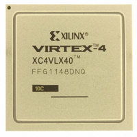
XC4VLX40-10FFG1148C Xilinx Inc, XC4VLX40-10FFG1148C Datasheet - Page 2

XC4VLX40-10FFG1148C
Manufacturer Part Number
XC4VLX40-10FFG1148C
Description
IC FPGA VIRTEX-4 40K 1148-FBGA
Manufacturer
Xilinx Inc
Series
Virtex™-4r
Specifications of XC4VLX40-10FFG1148C
Total Ram Bits
1769472
Number Of Logic Elements/cells
41472
Number Of Labs/clbs
4608
Number Of I /o
640
Voltage - Supply
1.14 V ~ 1.26 V
Mounting Type
Surface Mount
Operating Temperature
0°C ~ 85°C
Package / Case
1148-BBGA, FCBGA
No. Of Logic Blocks
4608
No. Of Macrocells
41472
Family Type
Virtex-4
No. Of Speed Grades
10
No. Of I/o's
640
Clock Management
DCM
Core Supply
RoHS Compliant
Lead Free Status / RoHS Status
Lead free / RoHS Compliant
Number Of Gates
-
Lead Free Status / RoHS Status
Lead free / RoHS Compliant
Other names
122-1491
Available stocks
Company
Part Number
Manufacturer
Quantity
Price
Company:
Part Number:
XC4VLX40-10FFG1148C
Manufacturer:
XILINX
Quantity:
1 238
Company:
Part Number:
XC4VLX40-10FFG1148C
Manufacturer:
Xilinx Inc
Quantity:
10 000
Part Number:
XC4VLX40-10FFG1148C
Manufacturer:
XILINX/赛灵思
Quantity:
20 000
Table 1: Absolute Maximum Ratings (Continued)
Table 2: Recommended Operating Conditions
DS302 (v3.7) September 9, 2009
Product Specification
Notes:
1.
2.
3.
4.
AVCCAUXMGT
V
AVCCAUXRX
AVCCAUXTX
CCO
Stresses beyond those listed under Absolute Maximum Ratings might cause permanent damage to the device. These are stress ratings only, and
functional operation of the device at these or any other conditions beyond those listed under Operating Conditions is not implied. Exposure to
Absolute Maximum Ratings conditions for extended periods of time might affect device reliability.
For soldering guidelines and thermal considerations, see the
When using more than 100 3.3V I/Os, refer to the
For more flexibility in specific designs, a maximum of 100 user I/Os can be stressed beyond the normal spec for no more than 20% of a data period.
There are no bank restrictions.
Symbol
V
Symbol
V
V
BATT
CCAUX
CCINT
V
T
T
V
V
V
I
(1,3,4,5)
IN
STG
SOL
T
TRX
TTX
IN
TS
J
(2)
Internal supply voltage relative to GND, T
Internal supply voltage relative to GND, T
Auxiliary supply voltage relative to GND, T
Auxiliary supply voltage relative to GND, T
Supply voltage relative to GND, T
Supply voltage relative to GND, T
3.3V supply voltage relative to GND, T
3.3V supply voltage relative to GND, T
2.5V and below supply voltage relative to GND,
T
2.5V and below supply voltage relative to GND,
T
Maximum current through any pin in a powered or unpowered
bank when forward biasing the clamp diode.
Battery voltage relative to GND, T
Battery voltage relative to GND, T
J
J
Voltage applied to 3-state 3.3V output
(all user and dedicated I/Os)
Voltage applied to 3-state 3.3V output
(restricted to maximum of 100 user I/Os)
2.5V or below I/O input voltage relative to GND
(user and dedicated I/Os)
Receive auxiliary supply voltage relative to analog ground, GNDA
(RocketIO pins)
Transmit auxiliary supply voltage relative to analog ground, GNDA
(RocketIO pins)
Management auxiliary supply voltage relative to analog ground, GNDA
(RocketIO pins)
Terminal receive supply voltage relative to GND
Terminal transmit supply voltage relative to GND
Storage temperature (ambient)
Maximum soldering temperature
Maximum junction temperature
= 0° C to +85° C
= –40° C to +100° C
Description
Virtex-4 FPGA User
Description
(2)
J
J
J
J
(2)
= 0° C to +85° C
= –40° C to +100° C
= 0° C to +85° C
= –40° C to +100° C
J
J
Virtex-4 Packaging and Pinout Specification
= 0° C to +85° C
= –40° C to +100° C
www.xilinx.com
J
J
J
J
(3,4)
= 0° C to +85° C
= –40° C to +100° C
= –40° C to +100° C
Virtex-4 FPGA Data Sheet: DC and Switching Characteristics
= 0° C to +85° C
Guide, Chapter 6, “3.3V I/O Design Guidelines.”
Commercial
Commercial
Commercial
Commercial
Commercial
Commercial
Commercial
Industrial
Industrial
Industrial
Industrial
Industrial
Industrial
Industrial
on the Xilinx website.
GND – 0.20
GND – 0.20
GND – 0.20
GND – 0.20
(Commercial Temperature)
(Industrial Temperature)
2.375
2.375
Min
1.14
1.14
1.14
1.14
–0.75 to V
1.0
1.0
–0.75 to 4.05
–0.85 to 4.3
–0.5 to 1.32
–0.5 to 1.32
–0.5 to 1.65
–0.95 to 4.4
–0.5 to 3.0
–0.5 to 3.0
–65 to 150
+220
+125
CCO
V
V
CCO
CCO
2.625
2.625
Max
1.26
1.26
3.45
3.45
3.45
3.45
3.6
3.6
+0.5
10
10
+ 0.2
+ 0.2
Units
Units
mA
mA
° C
° C
° C
V
V
V
V
V
V
V
V
V
V
V
V
V
V
V
V
V
V
V
V
2


