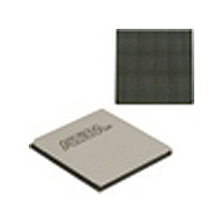
EP4SGX530HH35C2N Altera, EP4SGX530HH35C2N Datasheet - Page 53

EP4SGX530HH35C2N
Manufacturer Part Number
EP4SGX530HH35C2N
Description
IC STRATIX IV FPGA 530K 1152HBGA
Manufacturer
Altera
Series
Stratix® IV GXr
Datasheets
1.EP4SGX110DF29C3N.pdf
(80 pages)
2.EP4SGX110DF29C3N.pdf
(1154 pages)
3.EP4SGX110DF29C3N.pdf
(432 pages)
4.EP4SGX110DF29C3N.pdf
(22 pages)
5.EP4SGX110DF29C3N.pdf
(30 pages)
6.EP4SGX110DF29C3N.pdf
(72 pages)
7.EP4SGX530HH35C2N.pdf
(1145 pages)
Specifications of EP4SGX530HH35C2N
Number Of Logic Elements/cells
531200
Number Of Labs/clbs
21248
Total Ram Bits
27376
Number Of I /o
564
Voltage - Supply
0.87 V ~ 0.93 V
Mounting Type
Surface Mount
Operating Temperature
0°C ~ 85°C
Package / Case
1152-HBGA
Family Name
Stratix® IV
Number Of Logic Blocks/elements
531200
# Registers
424960
# I/os (max)
560
Process Technology
40nm
Operating Supply Voltage (typ)
900mV
Logic Cells
531200
Ram Bits
28033024
Operating Supply Voltage (min)
0.87V
Operating Supply Voltage (max)
0.93V
Operating Temp Range
0C to 85C
Operating Temperature Classification
Commercial
Mounting
Surface Mount
Pin Count
1152
Package Type
FCHBGA
Lead Free Status / RoHS Status
Lead free / RoHS Compliant
Number Of Gates
-
Lead Free Status / Rohs Status
Compliant
Available stocks
Company
Part Number
Manufacturer
Quantity
Price
Chapter 1: DC and Switching Characteristics for Stratix IV Devices
Switching Characteristics
Table 1–41. High-Speed I/O Specifications
April 2011 Altera Corporation
f
clock frequency)
True Differential I/O
Standards
f
clock frequency)
Single Ended I/O
Standards
f
clock frequency)
Single Ended I/O
Standards
f
clock frequency)
HSCLK_in
HSCLK_in
HSCLK_in
HSCLK_OUT
Symbol
(input
(input
(input
Periphery Performance
(output
(9)
(10)
1
Clock boost factor W = 1 to 40
Clock boost factor W = 1 to 40
Clock boost factor W = 1 to 40
Chip-Wide Reset (Dev_CLRn) Specifications
Table 1–40
Table 1–40. Chip-Wide Reset (DEV_CLRn) Specifications
This section describes periphery performance, including high-speed I/O and external
memory interface.
I/O performance supports several system interfaces, such as the LVDS high-speed
I/O interface, external memory interface, and the PCI/PCI-X bus interface.
General-purpose I/O standards such as 3.3-, 2.5-, 1.8-, and 1.5-LVTTL/LVCMOS are
capable of typical 167 MHz and 1.2 LVCMOS at 100 MHz interfacing frequency with
10 pF load.
Actual achievable frequency depends on design- and system-specific factors. You
must perform HSPICE/IBIS simulations based on your specific design and system
setup to determine the maximum achievable frequency in your system.
High-Speed I/O Specification
Table 1–41
Dev_CLRn
Conditions
—
(3)
(3)
(3)
lists the specifications for the Stratix IV chip-wide reset (Dev_CLRn).
lists the high-speed I/O timing for Stratix IV devices.
Description
(Note 1), (2), (10)
–2/–2× Speed Grade
Min
5
5
5
5
Typ
—
—
—
—
Stratix IV Device Handbook Volume 4: Device Datasheet and Addendum
(Part 1 of 3)—Preliminary
Min
500
Max
800
800
520
800
(7)
Min
5
5
5
5
–3
Speed Grade
Typ
Typ
—
—
—
—
—
Max
717
717
420
717
(7)
Max
—
Min
5
5
5
5
–4
Speed Grade
Typ
—
—
—
—
Unit
μs
Max
717
717
420
717
(7)
1–51
MHz
MHz
MHz
MHz
Unit


