XC3S50AN-4TQG144I Xilinx Inc, XC3S50AN-4TQG144I Datasheet - Page 53

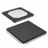
XC3S50AN-4TQG144I
Manufacturer Part Number
XC3S50AN-4TQG144I
Description
IC FPGA SPARTAN-3AN50K 144-TQFP
Manufacturer
Xilinx Inc
Series
Spartan™-3ANr
Datasheets
1.XC3S50A-4VQG100C.pdf
(7 pages)
2.XC3S50AN-4TQG144C.pdf
(2 pages)
3.XC3S50AN-4TQG144C.pdf
(123 pages)
Specifications of XC3S50AN-4TQG144I
Total Ram Bits
55296
Number Of Logic Elements/cells
1584
Number Of Labs/clbs
176
Number Of I /o
108
Number Of Gates
50000
Voltage - Supply
1.14 V ~ 1.26 V
Mounting Type
Surface Mount
Operating Temperature
-40°C ~ 100°C
Package / Case
144-LQFP
No. Of Logic Blocks
176
No. Of Gates
50000
No. Of Macrocells
1584
Family Type
Spartan-3AN
No. Of Speed Grades
4
No. Of I/o's
108
Clock
RoHS Compliant
Lead Free Status / RoHS Status
Lead free / RoHS Compliant
Other names
122-1597
XC3S50AN-4TQG144I
XC3S50AN-4TQG144I
Available stocks
Company
Part Number
Manufacturer
Quantity
Price
Company:
Part Number:
XC3S50AN-4TQG144I
Manufacturer:
XILINX
Quantity:
760
Company:
Part Number:
XC3S50AN-4TQG144I
Manufacturer:
XILINX
Quantity:
54
Company:
Part Number:
XC3S50AN-4TQG144I
Manufacturer:
XILINX
Quantity:
59
Company:
Part Number:
XC3S50AN-4TQG144I
Manufacturer:
Xilinx Inc
Quantity:
10 000
Part Number:
XC3S50AN-4TQG144I
Manufacturer:
XILINX/赛灵思
Quantity:
20 000
Table 40: Switching Characteristics for the DLL
DS557 (v4.1) April 1, 2011
Product Specification
CLKOUT_DUTY_CYCLE_DLL
Output Frequency Ranges
CLKOUT_FREQ_CLK0
CLKOUT_FREQ_CLK90
CLKOUT_FREQ_2X
CLKOUT_FREQ_DV
Output Clock Jitter
CLKOUT_PER_JITT_0
CLKOUT_PER_JITT_90
CLKOUT_PER_JITT_180
CLKOUT_PER_JITT_270
CLKOUT_PER_JITT_2X
CLKOUT_PER_JITT_DV1
CLKOUT_PER_JITT_DV2
Duty Cycle
Phase Alignment
CLKIN_CLKFB_PHASE
CLKOUT_PHASE_DLL
Lock Time
LOCK_DLL
Symbol
(3)
(4)
(4)
(2,3,4)
Frequency for the CLK0 and CLK180 outputs
Frequency for the CLK90 and CLK270 outputs
Frequency for the CLK2X and CLK2X180 outputs
Frequency for the CLKDV output
Period jitter at the CLK0 output
Period jitter at the CLKDV output when performing
integer division
Period jitter at the CLKDV output when performing
non-integer division
Duty cycle variation for the CLK0, CLK90, CLK180,
CLK270, CLK2X, CLK2X180, and CLKDV outputs,
including the BUFGMUX and clock tree duty-cycle
distortion
outputs
When using the DLL alone:
The time from deassertion at
the DCM’s Reset input to the
rising transition at its LOCKED
output. When the DCM is
locked, the CLKIN and CLKFB
signals are in phase
Period jitter at the CLK90 output
Period jitter at the CLK180 output
Period jitter at the CLK270 output
Period jitter at the CLK2X and CLK2X180 outputs
Phase offset between the CLKIN and CLKFB inputs
Phase offset between DLL
Description
www.xilinx.com
Spartan-3AN FPGA Family: DC and Switching Characteristics
5 MHz < F
F
(not CLK2X180)
CLK0 to CLK2X
CLKIN
All others
15 MHz
> 15 MHz
CLKIN
<
Device
All
All
All
All
All
0.3125
Min
10
5
5
–
–
–
–
–
–
–
–
–
–
–
–
–
-5
±[1% of
±[1% of
±[1% of
±[0.5%
±[0.5%
CLKIN
CLKIN
CLKIN
CLKIN
CLKIN
period
+ 100]
period
+ 100]
period
+ 350]
period
+ 100]
period
+ 150]
±100
±150
±150
±150
±150
±150
Speed Grade
Max
280
200
334
186
600
of
of
5
0.3125
Min
10
5
5
–
–
–
–
–
–
–
–
–
–
–
–
–
-4
±[1% of
±[1% of
±[1% of
±[0.5%
±[0.5%
CLKIN
CLKIN
CLKIN
CLKIN
CLKIN
period
+ 100]
period
+ 100]
period
+ 350]
period
+ 100]
period
+ 150]
±100
±150
±150
±150
±150
±150
Max
250
200
334
166
600
of
of
5
Units
MHz
MHz
MHz
MHz
ms
ps
ps
ps
ps
ps
ps
ps
ps
ps
ps
ps
µs
53


