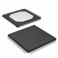
XC3S50AN-4TQG144I Xilinx Inc, XC3S50AN-4TQG144I Datasheet - Page 68

XC3S50AN-4TQG144I
Manufacturer Part Number
XC3S50AN-4TQG144I
Description
IC FPGA SPARTAN-3AN50K 144-TQFP
Manufacturer
Xilinx Inc
Series
Spartan™-3ANr
Datasheets
1.XC3S50A-4VQG100C.pdf
(7 pages)
2.XC3S50AN-4TQG144C.pdf
(2 pages)
3.XC3S50AN-4TQG144C.pdf
(123 pages)
Specifications of XC3S50AN-4TQG144I
Total Ram Bits
55296
Number Of Logic Elements/cells
1584
Number Of Labs/clbs
176
Number Of I /o
108
Number Of Gates
50000
Voltage - Supply
1.14 V ~ 1.26 V
Mounting Type
Surface Mount
Operating Temperature
-40°C ~ 100°C
Package / Case
144-LQFP
No. Of Logic Blocks
176
No. Of Gates
50000
No. Of Macrocells
1584
Family Type
Spartan-3AN
No. Of Speed Grades
4
No. Of I/o's
108
Clock
RoHS Compliant
Lead Free Status / RoHS Status
Lead free / RoHS Compliant
Other names
122-1597
XC3S50AN-4TQG144I
XC3S50AN-4TQG144I
Available stocks
Company
Part Number
Manufacturer
Quantity
Price
Company:
Part Number:
XC3S50AN-4TQG144I
Manufacturer:
XILINX
Quantity:
760
Company:
Part Number:
XC3S50AN-4TQG144I
Manufacturer:
XILINX
Quantity:
54
Company:
Part Number:
XC3S50AN-4TQG144I
Manufacturer:
XILINX
Quantity:
59
Company:
Part Number:
XC3S50AN-4TQG144I
Manufacturer:
Xilinx Inc
Quantity:
10 000
Part Number:
XC3S50AN-4TQG144I
Manufacturer:
XILINX/赛灵思
Quantity:
20 000
Table 61: Timing for the JTAG
DS557 (v4.1) April 1, 2011
Product Specification
Notes:
1.
2.
Clock-to-Output Times
T
Setup Times
T
T
Hold Times
T
T
Clock Timing
T
T
T
T
F
Symbol
TCKTDO
TDITCK
TMSTCK
TCKTDI
TCKTMS
CCH
CCL
CCHDNA
CCLDNA
TCK
The numbers in this table are based on the operating conditions set forth in
For details on JTAG, see Chapter 9, “JTAG Configuration Mode and Boundary-Scan” in
Guide.
The time from the falling transition on the TCK pin to data appearing at the TDO pin
The time from the setup of data at the
TDI pin to the rising transition at the
TCK pin
The time from the setup of a logic level at the TMS pin to the rising transition at the TCK pin
The time from the rising transition at
the TCK pin to the point when data is
last held at the TDI pin
The time from the rising transition at the TCK pin to the point when a logic level is last held at the
TMS pin
The High pulse width at the TCK pin
The Low pulse width at the TCK pin
The High pulse width at the TCK pin
The Low pulse width at the TCK pin
Frequency of the TCK signal
(2)
Test Access Port
All functions except ISC_DNA command
All devices and functions except those shown below
Boundary-Scan commands (INTEST, EXTEST,
SAMPLE) on XC3S700AN and XC3S1400AN FPGAs
All functions except those shown below
Configuration commands (CFG_IN, ISC_PROGRAM)
During ISC_DNA command
All operations on XC3S50AN, XC3S200AN, and
XC3S400AN FPGAs and for BYPASS or HIGHZ
instructions on all FPGAs
All operations on XC3S700AN and XC3S1400AN
FPGAs, except for BYPASS or HIGHZ instructions
Description
www.xilinx.com
Spartan-3AN FPGA Family: DC and Switching Characteristics
Table
10.
UG332
Spartan-3 Generation Configuration User
11.0
Min
1.0
7.0
7.0
2.0
10
10
0
0
5
5
0
All Speed
Grades
10,000
10,000
Max
11.0
33
20
–
–
–
–
–
–
Units
MHz
ns
ns
ns
ns
ns
ns
ns
ns
ns
68


