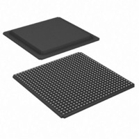
XC3SD3400A-5FG676C Xilinx Inc, XC3SD3400A-5FG676C Datasheet - Page 23

XC3SD3400A-5FG676C
Manufacturer Part Number
XC3SD3400A-5FG676C
Description
SPARTAN-3ADSP FPGA 3400K 676FBGA
Manufacturer
Xilinx Inc
Series
Spartan™-3A DSPr
Datasheets
1.XC3S50A-4VQG100C.pdf
(7 pages)
2.XC3SD3400A-4FGG676C.pdf
(4 pages)
3.XC3SD3400A-4FGG676C.pdf
(101 pages)
Specifications of XC3SD3400A-5FG676C
Number Of Logic Elements/cells
53712
Number Of Labs/clbs
5968
Total Ram Bits
2322432
Number Of I /o
469
Number Of Gates
3400000
Voltage - Supply
1.14 V ~ 1.26 V
Mounting Type
Surface Mount
Operating Temperature
0°C ~ 85°C
Package / Case
676-BBGA
For Use With
122-1532 - KIT DEVELOPMENT SPARTAN 3ADSP
Lead Free Status / RoHS Status
Contains lead / RoHS non-compliant
Available stocks
Company
Part Number
Manufacturer
Quantity
Price
Company:
Part Number:
XC3SD3400A-5FG676C
Manufacturer:
XILINX
Quantity:
885
Company:
Part Number:
XC3SD3400A-5FG676C
Manufacturer:
Xilinx Inc
Quantity:
10 000
Table 19: Setup and Hold Times for the IOB Input Path (Cont’d)
Table 20: Sample Window (Source Synchronous)
DS610 (v3.0) October 4, 2010
Product Specification
Notes:
1.
2.
3.
T
Set/Reset Pulse Width
T
Symbol
T
Symbol
IOICKPD
RPW_IOB
SAMP
The numbers in this table are tested using the methodology presented in
Table 7
This setup time requires adjustment whenever a signal standard other than LVCMOS25 is assigned to the data Input. If this is true, add the
appropriate Input adjustment from
These hold times require adjustment whenever a signal standard other than LVCMOS25 is assigned to the data Input. If this is true, subtract
the appropriate Input adjustment from
edge.
Setup and hold
capture window of
an IOB flip-flop.
and
Time from the active transition at the
ICLK input of the Input Flip-Flop (IFF) to
the point where data must be held at the
Input pin. The Input Delay is
programmed.
Minimum pulse width to SR control input
on IOB
Description
Table
10.
Description
The input capture sample window value is highly specific to a particular application, device,
package, I/O standard, I/O placement, DCM usage, and clock buffer. Please consult the
appropriate Xilinx Answer Record for application-specific values.
• Answer Record
Table
Table
22.
22. When the hold time is negative, it is possible to change the data before the clock’s active
30879
LVCMOS25
Conditions
Spartan-3A DSP FPGA Family: DC and Switching Characteristics
www.xilinx.com
–
(3)
Table 26
Max
DELAY_
VALUE
and are based on the operating conditions set forth in
1
2
3
4
5
6
7
8
1
2
3
4
5
6
7
8
–
XC3SD1800A –1.40 –1.40
XC3SD3400A –1.31 –1.31
Device
All
–2.11 –2.11
–2.48 –2.48
–2.77 –2.77
–2.62 –2.62
–3.06 –3.06
–3.42 –3.42
–3.65 –3.65
–1.88 –1.88
–2.44 –2.44
–2.89 –2.89
–2.83 –2.83
–3.33 –3.33
–3.63 –3.63
–3.96 –3.96
1.33
Min
-5
Speed
1.61
Min
-4
Units
Units
ns
ns
ns
ns
ns
ns
ns
ns
ns
ns
ns
ns
ns
ns
ns
ns
ns
ps
23


