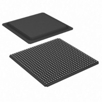
XC3SD3400A-5FG676C Xilinx Inc, XC3SD3400A-5FG676C Datasheet - Page 39

XC3SD3400A-5FG676C
Manufacturer Part Number
XC3SD3400A-5FG676C
Description
SPARTAN-3ADSP FPGA 3400K 676FBGA
Manufacturer
Xilinx Inc
Series
Spartan™-3A DSPr
Datasheets
1.XC3S50A-4VQG100C.pdf
(7 pages)
2.XC3SD3400A-4FGG676C.pdf
(4 pages)
3.XC3SD3400A-4FGG676C.pdf
(101 pages)
Specifications of XC3SD3400A-5FG676C
Number Of Logic Elements/cells
53712
Number Of Labs/clbs
5968
Total Ram Bits
2322432
Number Of I /o
469
Number Of Gates
3400000
Voltage - Supply
1.14 V ~ 1.26 V
Mounting Type
Surface Mount
Operating Temperature
0°C ~ 85°C
Package / Case
676-BBGA
For Use With
122-1532 - KIT DEVELOPMENT SPARTAN 3ADSP
Lead Free Status / RoHS Status
Contains lead / RoHS non-compliant
Available stocks
Company
Part Number
Manufacturer
Quantity
Price
Company:
Part Number:
XC3SD3400A-5FG676C
Manufacturer:
XILINX
Quantity:
885
Company:
Part Number:
XC3SD3400A-5FG676C
Manufacturer:
Xilinx Inc
Quantity:
10 000
Table 30: CLB Distributed RAM Switching Characteristics
Table 31: CLB Shift Register Switching Characteristics
DS610 (v3.0) October 4, 2010
Product Specification
Clock-to-Output Times
T
Setup Times
T
T
T
Hold Times
T
T
Clock Pulse Width
T
Clock-to-Output Times
T
Setup Times
T
Hold Times
T
Clock Pulse Width
T
AS
AH,
SHCKO
DS
WS
DH
WPH
REG
SRLDS
SRLDH
WPH
T
Symbol
Symbol
, T
, T
WH
WPL
WPL
Time from the active edge at the CLK input to data appearing on
the distributed RAM output
Setup time of data at the BX or BY input before the active
transition at the CLK input of the distributed RAM
Setup time of the F/G address inputs before the active transition
at the CLK input of the distributed RAM
Setup time of the write enable input before the active transition at
the CLK input of the distributed RAM
Hold time of the BX and BY data inputs after the active transition
at the CLK input of the distributed RAM
Hold time of the F/G address inputs or the write enable input after
the active transition at the CLK input of the distributed RAM
Minimum High or Low pulse width at CLK input
Time from the active edge at the CLK input to data appearing on
the shift register output
Setup time of data at the BX or BY input before the active
transition at the CLK input of the shift register
Hold time of the BX or BY data input after the active transition at
the CLK input of the shift register
Minimum High or Low pulse width at CLK input
Description
Description
Spartan-3A DSP FPGA Family: DC and Switching Characteristics
www.xilinx.com
–0.07
0.18
0.30
0.13
0.01
0.88
0.13
0.16
0.90
Min
Min
–
–
-5
-5
Speed Grade
Speed Grade
Max
1.44
Max
4.11
–
–
–
–
–
–
–
–
–
–0.02
0.36
0.59
0.13
0.01
1.01
0.18
0.16
1.01
Min
Min
–
–
-4
-4
Max
Max
1.72
4.82
–
–
–
–
–
–
–
–
–
Units
Units
ns
ns
ns
ns
ns
ns
ns
ns
ns
ns
ns
39


