DLP-HS-FPGA DLP Design Inc, DLP-HS-FPGA Datasheet - Page 10
DLP-HS-FPGA
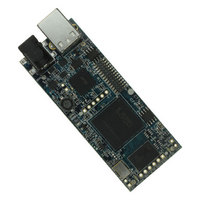
Manufacturer Part Number
DLP-HS-FPGA
Description
MODULE USB-TO-FPGA SPARTAN3
Manufacturer
DLP Design Inc
Datasheet
1.DLP-HS-FPGA.pdf
(17 pages)
Specifications of DLP-HS-FPGA
Module/board Type
FPGA Module
Interface Type
USB, SPI
Data Bus Width
32 bit
Operating Supply Voltage
5 V
Product
Interface Modules
For Use With/related Products
USB
Lead Free Status / RoHS Status
Lead free / RoHS Compliant
Lead Free Status / RoHS Status
Lead free / RoHS Compliant, Lead free / RoHS Compliant
Other names
813-1030
Available stocks
Company
Part Number
Manufacturer
Quantity
Price
Company:

Part Number:
DLP-HS-FPGA
Manufacturer:
DLP Design
Quantity:
135


The USER I/O Pin Read / Set / Clear commands I/O number mapping to the physical I/O pins on the
DLP-HS-FPGA board are described in the following table.
Rev. 1.1 (December 2009)
I/O Number
0x0C (12)
0x0D (13)
0x1C (28)
0x1D (29)
0x0A (10)
0x0B (11)
0x0E (14)
0x0F (15)
0x1A (26)
0x1B (27)
0x1E (30)
0x1F (31)
0x10 (16)
0x11 (17)
0x12 (18)
0x13 (19)
0x14 (20)
0x15 (21)
0x16 (22)
0x17 (23)
0x18 (24)
0x19 (25)
0x20 (32)
0x21 (33)
0x22 (34)
0x23 (35)
0x00 (0)
0x01 (1)
0x02 (2)
0x03 (3)
0x04 (4)
0x05 (5)
0x06 (6)
0x07 (7)
0x08 (8)
0x09 (9)
FPGA Pin
DLP-HS-
J1 pin 10
J1 pin 12
J1 pin 13
J1 pin 14
J1 pin 15
J1 pin 16
J1 pin 17
J1 pin 18
J1 pin 19
J1 pin 20
J1 pin 21
J1 pin 22
J1 pin 27
J1 pin 29
J1 pin 30
J1 pin 31
J1 pin 32
J1 pin 33
J1 pin 34
J1 pin 35
J1 pin 36
J1 pin 37
J1 pin 38
J1 pin 39
J1 pin 41
J1 pin 42
J1 pin 43
J1 pin 44
J1 pin 2
J1 pin 3
J1 pin 4
J1 pin 5
J1 pin 6
J1 pin 7
J1 pin 8
J1 pin 9
XC3S200A
D13
C13
D11
C12
C10
A14
A13
C11
A11
Pin
M4
D9
C8
D8
C5
G4
C2
C1
D1
H6
H5
N3
H3
A6
B6
B8
A8
A5
B3
A3
F3
E1
E3
E2
J6
J4
J3
XC3S200A
TABLE 2
User I/O
Bank
0
0
0
0
0
0
0
0
0
0
0
0
0
0
0
0
0
0
0
0
3
3
3
3
3
3
3
3
3
3
3
3
3
3
3
3
10
FPGA Pin Configurations available
Digital Input, Output, Differential Pair 0+
Digital Input, Output, Differential Pair 0-
Digital Input, Output, Differential Pair 1-
Digital Input, Output, Differential Pair 1+
Digital Input, Output, Differential Pair 2+,
Global Clock
Digital Input, Output, Differential Pair 2-,
Global Clock
Digital Input, Output, Differential Pair 3+,
Global Clock
Digital Input, Output, Differential Pair 3-,
Global Clock
Digital Input, Output, Differential Pair 4+
Digital Input, Output, Differential Pair 4-
Digital Input, Output, Differential Pair 5+
Digital Input, Output, Differential Pair 5-
Digital Input, Output, Differential Pair 6+
Digital Input, Output, Differential Pair 6-
Digital Input, Output, Differential Pair 7-,
Global Clock
Digital Input, Output, Differential Pair 7+,
Global Clock
Digital Input, Output, Differential Pair 8-
Digital Input, Output, Differential Pair 8+
Digital Input, Output, Differential Pair 9-
Digital Input, Output, Differential Pair 9+
Digital Input, Output, Differential Pair 10+
Digital Input, Output, Differential Pair 10-
Digital Input, Output, Differential Pair 11+
Digital Input, Output, Differential Pair 11-
Digital Input, Output, Differential Pair 12-
Digital Input, Output, Differential Pair 12+
Digital Input, Output, Differential Pair 13-
Digital Input, Output, Differential Pair 13+
Digital Input, Output, Differential Pair 14+
Digital Input, Output, Differential Pair 14-
Digital Input, Output, Differential Pair 15-
Digital Input, Output, Differential Pair 15+
Digital Input, Output, Differential Pair 16+
Digital Input, Output, Differential Pair 16-
Digital Input, Output, Differential Pair 17+
Digital Input, Output, Differential Pair 17-
© DLP Design, Inc.
Related parts for DLP-HS-FPGA
Image
Part Number
Description
Manufacturer
Datasheet
Request
R

Part Number:
Description:
Interface Modules & Development Tools USB FPGA Module w/ Xilinx XC3S400A
Manufacturer:
DLP Design Inc
Datasheet:

Part Number:
Description:
MODULE USB-TO-UART/FIFO HS 18DIP
Manufacturer:
DLP Design Inc
Datasheet:

Part Number:
Description:
MODULE USB-TO-TTL SRL UART CONV
Manufacturer:
DLP Design Inc
Datasheet:

Part Number:
Description:
MODULE USB-TO-TTL PARL FIFO CONV
Manufacturer:
DLP Design Inc
Datasheet:
Part Number:
Description:
KIT DEV DLP LIGHTCOMANDER
Manufacturer:
Logic
Datasheet:

Part Number:
Description:
MODULE DATA-ACQUISITION 8-CH
Manufacturer:
DLP Design Inc
Datasheet:

Part Number:
Description:
MODULE DATA-ACQUISITION 20-CH
Manufacturer:
DLP Design Inc
Datasheet:

Part Number:
Description:
RFID READER/WRITER SNGL-CH OEM
Manufacturer:
DLP Design Inc
Datasheet:

Part Number:
Description:
Interface Modules & Development Tools DLP-245PL PACKAGED w/CCS Compiler
Manufacturer:
DLP Design Inc

Part Number:
Description:
MODULE USB-MCU FT245RL W/16F877A
Manufacturer:
DLP Design Inc
Datasheet:

Part Number:
Description:
MODULE USB-TO-FPGA TRAINING TOOL
Manufacturer:
DLP Design Inc
Datasheet:

Part Number:
Description:
MODULE USB-MCU FT232R W/18F2410
Manufacturer:
DLP Design Inc
Datasheet:

Part Number:
Description:
MODULE USB-MCU FT245RL W/SX48
Manufacturer:
DLP Design Inc
Datasheet:

Part Number:
Description:
MODULE USB-MCU FT2232D W/16F877A
Manufacturer:
DLP Design Inc
Datasheet:

Part Number:
Description:
MOD USB-MCU FT245RL W/18LF8722
Manufacturer:
DLP Design Inc
Datasheet: