DLP-HS-FPGA DLP Design Inc, DLP-HS-FPGA Datasheet - Page 3
DLP-HS-FPGA
Manufacturer Part Number
DLP-HS-FPGA
Description
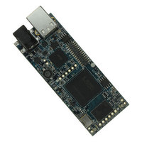
MODULE USB-TO-FPGA SPARTAN3
Manufacturer
DLP Design Inc
Datasheet
1.DLP-HS-FPGA.pdf
(17 pages)
Specifications of DLP-HS-FPGA
Module/board Type
FPGA Module
Interface Type
USB, SPI
Data Bus Width
32 bit
Operating Supply Voltage
5 V
Product
Interface Modules
For Use With/related Products
USB
Lead Free Status / RoHS Status
Lead free / RoHS Compliant
Lead Free Status / RoHS Status
Lead free / RoHS Compliant, Lead free / RoHS Compliant
Other names
813-1030
Available stocks
Company
Part Number
Manufacturer
Quantity
Price
Company:

Part Number:
DLP-HS-FPGA
Manufacturer:
DLP Design
Quantity:
135


2.0 REFERENCE DESIGN
A 10,000 line reference design is available for the Spartan™ 3A FPGA on the DLP-HS-FPGA to those
that purchase the module. The design was written in VHDL and built using the free Xilinx ISE™
WebPACK™ tools. The reference design consists of the following blocks:
It contains a USB interface block, a User I/0 block, a DDR2 SDRAM interface, a Heartbeat pulse
generator, and a clock generator. The SPI Flash is used to store the design’s FPGA configuration file.
The USB interface captures, interprets, and returns command and data information sent from the host
PC through the FTDI USB interface to the FPGA. Commands include ping, return status, loopback
data, set a User I/O pin high or low, read a User I/O pin, initialize the DDR2 SDRAM memory, and
read or write the DDR2 SDRAM memory. Section 10 explains these in detail.
The User I/O block controls access to the 63 User I/O pins accessible through the top and bottom side
headers. Every one of these pins can be either an input or an output. The User I/O block can
configure these pins as inputs and read their state, or as outputs and drive them high or low. As a side
note 48 of these User I/O pins can be configured as 24 differential pairs, 8 can be configured as
global clock inputs, and 6 can be configured as regional clock inputs.
The DDR2 SDRAM interface block manages the memory’s initialization, the refresh cycle, and the
read and write access. Read and write access is available in 4 byte bursts. The traces between the
DDR2 SDRAM and FPGA are matched within 10 mils to accommodate reliable data transfer at 266
Mbit/s (clocked at 133MHz). The interface creates and aligns the Data Strobes (DQS) based on an
external feedback trace that matches two times the trace length between the FPGA and the DDR2
SDRAM. The initialization, read, and write commands are initiated by the USB interface block, and
executed by the DDR2 SDRAM interface block.
The Heartbeat pulse generator takes the internal system clock and divides it down so that the on
board Heartbeat LED will be turned on and off at a duration of approximately one half second.
The clock generator block receives the 66 MHz clock, and produces both the 133 MHz clocks
required to run the DDR2 SDRAM memory device, and the 100 MHz clock for the remaining internal
logic in the FPGA. It also handles reset and lock synchronization between internal DCM blocks.
Rev. 1.1 (December 2009)
3
© DLP Design, Inc.
Related parts for DLP-HS-FPGA
Image
Part Number
Description
Manufacturer
Datasheet
Request
R

Part Number:
Description:
Interface Modules & Development Tools USB FPGA Module w/ Xilinx XC3S400A
Manufacturer:
DLP Design Inc
Datasheet:

Part Number:
Description:
MODULE USB-TO-UART/FIFO HS 18DIP
Manufacturer:
DLP Design Inc
Datasheet:

Part Number:
Description:
MODULE USB-TO-TTL SRL UART CONV
Manufacturer:
DLP Design Inc
Datasheet:

Part Number:
Description:
MODULE USB-TO-TTL PARL FIFO CONV
Manufacturer:
DLP Design Inc
Datasheet:
Part Number:
Description:
KIT DEV DLP LIGHTCOMANDER
Manufacturer:
Logic
Datasheet:

Part Number:
Description:
MODULE DATA-ACQUISITION 8-CH
Manufacturer:
DLP Design Inc
Datasheet:

Part Number:
Description:
MODULE DATA-ACQUISITION 20-CH
Manufacturer:
DLP Design Inc
Datasheet:

Part Number:
Description:
RFID READER/WRITER SNGL-CH OEM
Manufacturer:
DLP Design Inc
Datasheet:

Part Number:
Description:
Interface Modules & Development Tools DLP-245PL PACKAGED w/CCS Compiler
Manufacturer:
DLP Design Inc

Part Number:
Description:
MODULE USB-MCU FT245RL W/16F877A
Manufacturer:
DLP Design Inc
Datasheet:

Part Number:
Description:
MODULE USB-TO-FPGA TRAINING TOOL
Manufacturer:
DLP Design Inc
Datasheet:

Part Number:
Description:
MODULE USB-MCU FT232R W/18F2410
Manufacturer:
DLP Design Inc
Datasheet:

Part Number:
Description:
MODULE USB-MCU FT245RL W/SX48
Manufacturer:
DLP Design Inc
Datasheet:

Part Number:
Description:
MODULE USB-MCU FT2232D W/16F877A
Manufacturer:
DLP Design Inc
Datasheet:

Part Number:
Description:
MOD USB-MCU FT245RL W/18LF8722
Manufacturer:
DLP Design Inc
Datasheet: