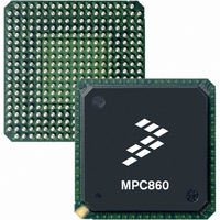
MPC859TVR133A Freescale Semiconductor, MPC859TVR133A Datasheet - Page 16

MPC859TVR133A
Manufacturer Part Number
MPC859TVR133A
Description
IC MPU POWERQUICC 133MHZ 357PBGA
Manufacturer
Freescale Semiconductor
Datasheet
1.MPC859DSLCVR50A.pdf
(96 pages)
Specifications of MPC859TVR133A
Processor Type
MPC8xx PowerQUICC 32-Bit
Speed
133MHz
Voltage
1.8V
Mounting Type
Surface Mount
Package / Case
357-PBGA
Processor Series
MPC8xx
Core
MPC8xx
Data Bus Width
32 bit
Maximum Clock Frequency
133 MHz
Maximum Operating Temperature
+ 95 C
Mounting Style
SMD/SMT
Minimum Operating Temperature
0 C
Family Name
MPC8xx
Device Core
PowerQUICC
Device Core Size
32b
Frequency (max)
133MHz
Instruction Set Architecture
RISC
Supply Voltage 1 (typ)
1.8V
Operating Supply Voltage (max)
1.9V
Operating Supply Voltage (min)
1.7V
Operating Temp Range
0C to 95C
Operating Temperature Classification
Commercial
Mounting
Surface Mount
Pin Count
357
Package Type
BGA
Lead Free Status / RoHS Status
Lead free / RoHS Compliant
Features
-
Lead Free Status / Rohs Status
Lead free / RoHS Compliant
Available stocks
Company
Part Number
Manufacturer
Quantity
Price
Company:
Part Number:
MPC859TVR133A
Manufacturer:
MOTOLOLA
Quantity:
1 045
Company:
Part Number:
MPC859TVR133A
Manufacturer:
Freescale Semiconductor
Quantity:
10 000
Bus Signal Timing
This recommendation particularly applies to the address and data buses. Maximum PC trace lengths of 6” are
recommended. Capacitance calculations should consider all device loads as well as parasitic capacitances due to the
PC traces. Attention to proper PCB layout and bypassing becomes especially critical in systems with higher
capacitive loads because these loads create higher transient currents in the V
inputs or signals that will be inputs during reset. Special care should be taken to minimize the noise levels on the
PLL supply pins. For more information, please refer to Section 14.4.3, Clock Synthesizer Power (VDDSYN,
VSSSYN, VSSSYN1), in the MPC866 User’s Manual.
10 Bus Signal Timing
The maximum bus speed supported by the MPC866/859 is 66 MHz. Higher-speed parts must be operated in
half-speed bus mode (for example, an MPC866/859 used at 100 MHz must be configured for a 50-MHz bus).
Table 7
Table 9
MPC866/859 bus shown in this table assumes a 50-pF load for maximum delays and a 0-pF load for minimum
delays. CLKOUT assumes a 100-pF load maximum delay.
16
Core
Bus
Num
Core
Bus
B1a EXTCLK to CLKOUT phase skew
B1b CLKOUT frequency jitter peak-to-peak
B1c
B1
Freq
Part
and
shows the timings for the MPC866/859 at 33, 40, 50, and 66 MHz bus operation. The timing for the
Part Freq
Bus Period (CLKOUT) See
Frequency jitter on EXTCLK
Table 8
Table 7. Frequency Ranges for Standard Part Frequencies (1:1 Bus Mode)
Table 8. Frequency Ranges for Standard Part Frequencies (2:1 Bus Mode)
Min
40
20
show the frequency ranges for standard part frequencies.
Characteristic
50 MHz
Max
50
25
Min
MPC866/MPC859 Hardware Specifications, Rev. 2
40
40
Table 7
Table 9. Bus Operation Timings
50 MHz
Min
40
20
66 MHz
Min
– 2
—
—
—
33 MHz
66.67
33.33
Max
Max
50
50
Max
0.50
+2
—
1
Min
– 2
—
—
—
40 MHz
Min
40
20
100 MHz
Max
0.50
+2
—
1
DD
Min
40
40
Min
and GND circuits. Pull up all unused
– 2
Max
—
—
—
100
50
50 MHz
Max
0.50
66 MHz
+2
—
1
Min
40
20
Freescale Semiconductor
Min
– 2
—
—
—
133 MHz
66 MHz
66.67
66.67
Max
Max
0.50
+2
—
1
133.34
66.67
Max
Unit
ns
ns
ns
%


