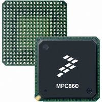
MPC859TVR133A Freescale Semiconductor, MPC859TVR133A Datasheet - Page 17

MPC859TVR133A
Manufacturer Part Number
MPC859TVR133A
Description
IC MPU POWERQUICC 133MHZ 357PBGA
Manufacturer
Freescale Semiconductor
Datasheet
1.MPC859DSLCVR50A.pdf
(96 pages)
Specifications of MPC859TVR133A
Processor Type
MPC8xx PowerQUICC 32-Bit
Speed
133MHz
Voltage
1.8V
Mounting Type
Surface Mount
Package / Case
357-PBGA
Processor Series
MPC8xx
Core
MPC8xx
Data Bus Width
32 bit
Maximum Clock Frequency
133 MHz
Maximum Operating Temperature
+ 95 C
Mounting Style
SMD/SMT
Minimum Operating Temperature
0 C
Family Name
MPC8xx
Device Core
PowerQUICC
Device Core Size
32b
Frequency (max)
133MHz
Instruction Set Architecture
RISC
Supply Voltage 1 (typ)
1.8V
Operating Supply Voltage (max)
1.9V
Operating Supply Voltage (min)
1.7V
Operating Temp Range
0C to 95C
Operating Temperature Classification
Commercial
Mounting
Surface Mount
Pin Count
357
Package Type
BGA
Lead Free Status / RoHS Status
Lead free / RoHS Compliant
Features
-
Lead Free Status / Rohs Status
Lead free / RoHS Compliant
Available stocks
Company
Part Number
Manufacturer
Quantity
Price
Company:
Part Number:
MPC859TVR133A
Manufacturer:
MOTOLOLA
Quantity:
1 045
Company:
Part Number:
MPC859TVR133A
Manufacturer:
Freescale Semiconductor
Quantity:
10 000
Freescale Semiconductor
B11a CLKOUT to TA, BI assertion (when
Num
B1d CLKOUT phase jitter peak-to-peak
B7a CLKOUT to TSIZ(0:1), REG, RSV,
B7b CLKOUT to BR, BG, FRZ, VFLS(0:1),
B8a CLKOUT to TSIZ(0:1), REG, RSV,
B8b CLKOUT to BR, BG, VFLS(0:1),
B11 CLKOUT to TS, BB assertion (MAX =
B12 CLKOUT to TS, BB negation (MAX =
B2
B3
B4
B5
B7
B8
B9
for OSCLK ≥ 15 MHz
CLKOUT phase jitter peak-to-peak
for OSCLK < 15 MHz
CLKOUT pulse width low (MIN = 0.4 x
B1, MAX = 0.6 x B1)
CLKOUT pulse width high (MIN = 0.4 x
B1, MAX = 0.6 x B1)
CLKOUT rise time
CLKOUT fall time
CLKOUT to A(0:31), BADDR(28:30),
RD/WR, BURST, D(0:31), DP(0:3)
output hold (MIN = 0.25 x B1)
AT(0:3), BDIP , PTR output hold (MIN =
0.25 x B1)
VF(0:2), IWP(0:2), LWP(0:1), STS
output hold (MIN = 0.25 x B1)
CLKOUT to A(0:31), BADDR(28:30)
RD/WR, BURST, D(0:31), DP(0:3),
valid (MAX = 0.25 x B1 + 6.3)
AT(0:3), BDIP, PTR valid (MAX = 0.25
x B1 + 6.3)
VF(0:2), IWP(0:2), FRZ, LWP(0:1),
STS valid
CLKOUT to A(0:31), BADDR(28:30),
RD/WR, BURST, D(0:31), DP(0:3),
TSIZ(0:1), REG, RSV, AT(0:3), PTR
High-Z (MAX = 0.25 x B1 + 6.3)
0.25 x B1 + 6.0)
driven by the memory controller or
PCMCIA interface) (MAX = 0.00 x B1 +
9.30
0.25 x B1 + 4.8)
1
)
4
Characteristic
(MAX = 0.25 x B1 + 6.3)
MPC866/MPC859 Hardware Specifications, Rev. 2
Table 9. Bus Operation Timings (continued)
12.1
12.1
7.60
7.60
7.60
7.60
7.60
2.50
7.60
Min
—
—
—
—
—
—
—
33 MHz
13.80
13.80
13.80
13.80
13.60
12.30
Max
18.2
18.2
4.00
4.00
9.30
—
—
—
4
5
10.0
10.0
6.30
6.30
6.30
6.30
6.30
2.50
6.30
Min
—
—
—
—
—
—
—
40 MHz
12.50
12.50
12.50
12.50
12.30
11.00
Max
15.0
15.0
4.00
4.00
9.30
—
—
—
4
5
5.00
5.00
5.00
5.00
5.00
2.50
5.00
Min
8.0
8.0
—
—
—
—
—
—
—
50 MHz
11.30
11.30
11.30
11.30
11.00
Max
12.0
12.0
4.00
4.00
9.30
9.80
—
—
—
4
5
3.80
3.80
3.80
3.80
3.80
2.50
3.80
Min
6.1
6.1
—
—
—
—
—
—
—
66 MHz
Bus Signal Timing
10.00
10.00
10.00
10.00
Max
4.00
9.80
9.80
8.50
4.00
9.1
9.1
—
—
—
4
5
Unit
ns
ns
ns
ns
ns
ns
ns
ns
ns
ns
ns
ns
ns
ns
ns
ns
17


