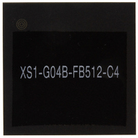
XS1-G04B-FB512-C4 XMOS, XS1-G04B-FB512-C4 Datasheet - Page 17

XS1-G04B-FB512-C4
Manufacturer Part Number
XS1-G04B-FB512-C4
Description
IC MPU 32BIT QUAD CORE 512FBGA
Manufacturer
XMOS
Datasheet
1.XS1-G04B-FB512-C4.pdf
(30 pages)
Specifications of XS1-G04B-FB512-C4
Processor Type
XCore 32-Bit
Speed
1600MIPS
Voltage
0.95 V ~ 1.05 V
Mounting Type
Surface Mount
Package / Case
512-BGA
For Use With
XMOS AVB REF KIT - KIT REF AVB W/4 XS1-G-DK880-1016 - KIT REF LED RGB 16X32 W/XC-3880-1015 - BOARD KIT XS1-G4 LED CTRL TILE880-1014 - BOARD DEV KIT XS1-G4 ETHERNET880-1013 - BOARD DEV KIT XS1-G4880-1012 - KIT DEV 4CORE G4 W/LCD TOUCH
Lead Free Status / RoHS Status
Lead free / RoHS Compliant
Features
-
Other names
880-1010
Available stocks
Company
Part Number
Manufacturer
Quantity
Price
XS1-G4 512BGA Datasheet (3.5)
A set of system clock dividers are applied to the system clock frequency allowing
The XS1-G4 has a total of 256K bytes of fast internal static memory for high rates
The OTP may be programmed using its internal charge pump or by supplying a
specific clock frequencies to be derived for each XCore, the switch and the reference
clock.
Clock edges must be monotonic and remain within the specified voltage and time
limits.
3.7 Memory
3.7.1 Internal static memory
of data throughput, divided into 64k bytes per XCore. Each internal memory access
consumes one core clock cycle. There is no dedicated external memory interface,
although memory can be expanded through appropriate use of the ports.
3.7.2 Internal one-time programmable memory
Each XCore has 64K bits of one-time programmable memory that can be programmed
using the JTAG interface.
3.7.3 OTP voltage ramp requirement
6.5V VPP programming voltage on the OTP_VPP pin. Unless a programming cycle is
underway the OTP_VPP pins should be left undriven.
For further information on security and OTP programming, see the relevant applica-
tion note.
3.8 Port Timing
Ports timing is explained in a separate application note. Please see
http://xmos.com/documentation
Symbol
Symbol
V(PP)
1. Clock frequencies between 20 and 25 MHz are not supported.
Parameter
System Clock Frequency
Parameter
OTP VPP Programming Volt-
age Ramp Rate
www.xmos.com
for more details.
MIN
MIN
TYP
TYP
MAX
400
MAX
1
UNITS
MHz
UNITS
V/ s
Notes
Notes
17/30


