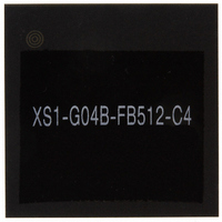
XS1-G04B-FB512-C4 XMOS, XS1-G04B-FB512-C4 Datasheet - Page 9

XS1-G04B-FB512-C4
Manufacturer Part Number
XS1-G04B-FB512-C4
Description
IC MPU 32BIT QUAD CORE 512FBGA
Manufacturer
XMOS
Datasheet
1.XS1-G04B-FB512-C4.pdf
(30 pages)
Specifications of XS1-G04B-FB512-C4
Processor Type
XCore 32-Bit
Speed
1600MIPS
Voltage
0.95 V ~ 1.05 V
Mounting Type
Surface Mount
Package / Case
512-BGA
For Use With
XMOS AVB REF KIT - KIT REF AVB W/4 XS1-G-DK880-1016 - KIT REF LED RGB 16X32 W/XC-3880-1015 - BOARD KIT XS1-G4 LED CTRL TILE880-1014 - BOARD DEV KIT XS1-G4 ETHERNET880-1013 - BOARD DEV KIT XS1-G4880-1012 - KIT DEV 4CORE G4 W/LCD TOUCH
Lead Free Status / RoHS Status
Lead free / RoHS Compliant
Features
-
Other names
880-1010
Available stocks
Company
Part Number
Manufacturer
Quantity
Price
XS1-G4 512BGA Datasheet (3.5)
These signals control the PLL of the XS1-G4
2 System Services
System Services are required to support correct device behavior. These signals
control clocking, reset and boot behavior of the device.
2.1 Clock control signals
Functional description
SS_EXT_OSC_CONFIG The on-chip PLL derives the system clock for the device by
SS_EXT_OSC_HS_MODE When SS_EXT_OSC_CONFIG is set high, this pin must be
SS_PLL_BYPASS When pin is set high, SS_CLK is used as the system clock. Set to
SS_BYPASS_PLL_LOCK Reserved, connect to ground.
Signal
SS_EXT_OSC_CONFIG
SS_EXT_OSC_HS_MODE
SS_PLL_BYPASS
SS_BYPASS_PLL_LOCK
SS_PLL_AVDD
SS_PLL_AGND
SS_CLK
multiplication of the input reference on SS_CLK. By default this ratio is set to
multiply by 20, giving an internal operating frequency of 400MHz. Achieving a
very specific core frequency requires a different reference frequency on SS_CLK.
If the SS_CLK frequency is not 20 MHz, this pin should be tied to VDD. See the
XS1-G Clock Frequency Control Application Note
driven low if the SS_CLK reference frequency is below 50MHz or driven high
if the reference frequency is above 50 MHz. This configuration is used to
configure the PLL such that the device boots up at a frequency that is not in
excess of 400MHz. See the
for further information.
IO_VDD.
Ball ID
M7
N7
G8
G9
H7
www.xmos.com
XS1-G Clock Frequency Control Application Note
I/O
I, PD
I, PD
I, PD
I, PD
pwr
pwr
I, PD, ST
Function Description
Control
Control
Control
Control
Clock
for further information.
PLL input oscillator configura-
tion mode
PLL input oscillator high speed
mode
Bypasses the PLL, using SS_CLK
directly
Reserved, connect to ground
Analog power supply to the PLL
AGND power supply for the PLL
System clock
9/30


