GC80503CSM66166SL388 Intel, GC80503CSM66166SL388 Datasheet - Page 26
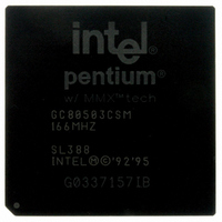
GC80503CSM66166SL388
Manufacturer Part Number
GC80503CSM66166SL388
Description
IC MPU 1.9V PENTI 166MHZ 352BGA
Manufacturer
Intel
Datasheet
1.GC80503CSM66166SL388.pdf
(62 pages)
Specifications of GC80503CSM66166SL388
Rohs Status
RoHS non-compliant
Processor Type
Pentium I w/MMX
Features
66MHz Bus
Speed
166MHz
Voltage
1.9V
Mounting Type
Surface Mount
Package / Case
352-BGA
Other names
821225


Low-Power Embedded Pentium
26
Table 6.
Quick Pin Reference (Sheet 4 of 6)
IGNNE#
INIT
INTR
INV
KEN#
LOCK#
M/IO#
NA#
NMI
PCD
PCHK#
Symbol
Type
O
O
O
O
I
I
I
I
I
I
I
®
Processor with MMX™ Technology
This is the ignore numeric error input. This pin has no effect when the NE bit in
CR0 is set to 1. When the CR0.NE bit is 0, and the IGNNE# pin is asserted, the
processor will ignore any pending unmasked numeric exception and continue
executing floating-point instructions for the entire duration that this pin is asserted.
When the CR0.NE bit is 0, IGNNE# is not asserted, a pending unmasked numeric
exception exists (SW.ES = 1), and the floating-point instruction is one of FINIT,
FCLEX, FSTENV, FSAVE, FSTSW, FSTCW, FENI, FDISI, or FSETPM, the
processor will execute the instruction in spite of the pending exception. When the
CR0.NE bit is 0, IGNNE# is not asserted, a pending unmasked numeric exception
exists (SW.ES = 1), and the floating-point instruction is one other than FINIT,
FCLEX, FSTENV, FSAVE, FSTSW, FSTCW, FENI, FDISI, or FSETPM, the
processor will stop execution and wait for an external interrupt.
The processor initialization input pin forces the processor to begin execution in a
known state. The processor state after INIT is the same as the state after RESET
except that the internal caches, write buffers, and floating-point registers retain the
values they had prior to INIT. INIT may NOT be used in lieu of RESET after power
up.
If INIT is sampled high when RESET transitions from high to low, the processor will
perform built-in self test prior to the start of program execution.
An active maskable interrupt input indicates that an external interrupt has been
generated. If the IF bit in the EFLAGS register is set, the processor will generate
two locked interrupt acknowledge bus cycles and vector to an interrupt handler after
the current instruction execution is completed. INTR must remain active until the
first interrupt acknowledge cycle is generated to assure that the interrupt is
recognized.
The invalidation input determines the final cache line state (S or I) in case of an
inquire cycle hit. It is sampled together with the address for the inquire cycle in the
clock EADS# is sampled active.
The cache enable pin is used to determine whether the current cycle is cacheable
or not and is consequently used to determine cycle length. When the processor
generates a cycle that can be cached (CACHE# asserted) and KEN# is active, the
cycle will be transformed into a burst line fill cycle.
The bus lock pin indicates that the current bus cycle is locked. The processor will
not allow a bus hold when LOCK# is asserted (but AHOLD and BOFF# are
allowed). LOCK# goes active in the first clock of the first locked bus cycle and goes
inactive after the BRDY# is returned for the last locked bus cycle. LOCK# is
guaranteed to be de-asserted for at least one clock between back-to-back locked
cycles.
The memory/input-output is one of the primary bus cycle definition pins. It is
driven valid in the same clock as the ADS# signal is asserted. M/IO# distinguishes
between memory and I/O cycles.
An active next address input indicates that the external memory system is ready to
accept a new bus cycle although all data transfers for the current cycle have not yet
completed. The processor will issue ADS# for a pending cycle two clocks after NA#
is asserted. The processor supports up to two outstanding bus cycles.
The non-maskable interrupt request signal indicates that an external non-
maskable interrupt has been generated.
The page cache disable pin reflects the state of the PCD bit in CR3; Page
Directory Entry or Page Table Entry. The purpose of PCD is to provide an external
cacheability indication on a page-by-page basis.
The parity check output indicates the result of a parity check on a data read. It is
driven with parity status two clocks after BRDY# is returned. PCHK# remains low
one clock for each clock in which a parity error was detected. Parity is checked only
for the bytes on which valid data is returned.
Name and Function
Datasheet
Related parts for GC80503CSM66166SL388
Image
Part Number
Description
Manufacturer
Datasheet
Request
R

Part Number:
Description:
Microprocessor: Intel Celeron M Processor 320 and Ultra Low Voltage Intel Celeron M Processor at 600MHz
Manufacturer:
Intel Corporation
Part Number:
Description:
Intel 82550 Fast Ethernet Multifunction PCI/CardBus Controller
Manufacturer:
Intel Corporation
Datasheet:
Part Number:
Description:
Intel StrataFlash memory 32 Mbit. Access speed 120 ns
Manufacturer:
Intel Corporation
Datasheet:
Part Number:
Description:
Intel StrataFlash memory 32 Mbit. Access speed 120 ns
Manufacturer:
Intel Corporation
Datasheet:
Part Number:
Description:
Intel StrataFlash memory 64 Mbit. Access speed 150 ns
Manufacturer:
Intel Corporation
Datasheet:
Part Number:
Description:
Intel StrataFlash memory 32 Mbit. Access speed 100 ns
Manufacturer:
Intel Corporation
Datasheet:
Part Number:
Description:
DA28F640J5A-1505 Volt Intel StrataFlash Memory
Manufacturer:
Intel Corporation
Datasheet:
Part Number:
Description:
5 Volt Intel StrataFlash?? Memory
Manufacturer:
Intel Corporation
Datasheet:
Part Number:
Description:
5 Volt Intel StrataFlash?? Memory
Manufacturer:
Intel Corporation
Part Number:
Description:
Intel 6300ESB I/O Controller Hub
Manufacturer:
Intel Corporation
Datasheet:
Part Number:
Description:
Intel 82801DB I/O Controller Hub (ICH4), Pb-Free SLI
Manufacturer:
Intel Corporation
Datasheet:
Part Number:
Description:
Intel 82801FB I/O Controller Hub (ICH6)
Manufacturer:
Intel Corporation
Datasheet:
Part Number:
Description:
Intel Strataflash Memory28F128J3 28F640J3 28F320J3
Manufacturer:
Intel Corporation
Datasheet:
Part Number:
Description:
Controllers, Intel 430TX PCIset: 82439TX System Controller (MTXC)
Manufacturer:
Intel Corporation