GC80503CSM66166SL388 Intel, GC80503CSM66166SL388 Datasheet - Page 50
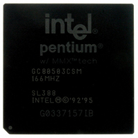
GC80503CSM66166SL388
Manufacturer Part Number
GC80503CSM66166SL388
Description
IC MPU 1.9V PENTI 166MHZ 352BGA
Manufacturer
Intel
Datasheet
1.GC80503CSM66166SL388.pdf
(62 pages)
Specifications of GC80503CSM66166SL388
Rohs Status
RoHS non-compliant
Processor Type
Pentium I w/MMX
Features
66MHz Bus
Speed
166MHz
Voltage
1.9V
Mounting Type
Surface Mount
Package / Case
352-BGA
Other names
821225


Low-Power Embedded Pentium
50
Table 24. APIC AC Specifications
Table 25. Notes to Tables 23 and 24
t
t
t
t
t
t
t
t
t
10.When driven asynchronously, RESET, NMI, FLUSH#, R/S#, INIT, and SMI# must be de-asserted (inactive)
12.BF2–BF0 should be strapped to V
13.Referenced to TCK falling edge.
14.1 ns can be added to the maximum TCK rise and fall times for every 10 MHz of frequency below 33 MHz.
15.Referenced to TCK rising edge.
16.Non-test outputs and inputs are the normal output or input signals (besides TCK, TRST#, TDI, TDO, and
17.During probe mode operation, do not use the boundary scan timings (t
18.This assumes an external pull-up resistor to V
19.The CLK to PICCLK ratio has to be an integer and the ratio (CLK/PICCLK) cannot be smaller than 4.
11. To guarantee proper asynchronous recognition, the signal must have been de-asserted (inactive) for a
Symbol
60a
60b
60c
60d
60e
60f
60g
60h
60i
t
t
t
t
1. CLK input frequency must be either 33.33 MHz (+1 MHz) or 66.6 MHz (–1 MHz). Operation in the range
2. Not 100 percent tested. Guaranteed by design.
3. These signals are measured on the rising edge of adjacent CLKs at V
4. 0.87 V/ns
5. APCHK#, FERR#, HLDA, IERR#, LOCK#, and PCHK# are glitch-free outputs. Glitch-free signals
6. Timing (t
7. Setup time is required to guarantee recognition on a specific clock.
8. This input may be driven asynchronously.
9. Hold time is required to guarantee recognition on a specific clock.
60j
61
62
63
between 33.33 MHz and 66.6 MHz is not supported.
relationship between the amplitude of the input jitter and the internal and external clocks, the jitter
frequency spectrum should not have any power spectrum peaking between 500 KHz and 1/3 of the CLK
operating frequency. The amount of jitter present must be accounted for as a component of CLK skew
between devices. The internal clock generator requires a constant frequency CLK input to within +250 ps,
and therefore the CLK input cannot be changed dynamically.
monotonically transition without false transitions.
active).
for a minimum of two clocks before being returned active.
minimum of two clocks before being returned active and must meet the minimum pulse width.
TMS). These timings correspond to the response of these signals due to boundary scan operations.
between 300
be between 6 ns and 36 ns.
PICCLK Frequency
PICCLK Period
PICCLK High Time
PICCLK Low Time
PICCLK Rise Time
PICCLK Fall Time
PICD0–1 Setup Time
PICD0–1 Hold Time
PICD0–1 Valid Delay (L to H)
PICD0–1 High Time (H to L)
PICCLK Setup Time
PICCLK Hold Time
PICCLK Ratio
(CLK/PICCLK)
14
) is required for external snooping (e.g., address setup to the CLK in which EADS# is sampled
CLK input rise/fall time
and 1 K , the capacitance must be between 20 pF and 120 pF, and the RC product must
Parameter
®
Processor with MMX™ Technology
CC3
8.7 V/ns.
or V
0.15
0.15
Min
SS
2.5
5.0
2.0
60
15
15
2
3
4
4
4
.
CC
and a lumped capacitive load. The pull-up resistor must be
16.66
Max
500
2.5
2.5
38
22
MHz
Unit
ns
ns
ns
ns
ns
ns
ns
ns
ns
CC3
55
Figure
–t
/V
58
13
13
13
13
13
16
16
14
14
16
16
CC2
).
. To ensure a 1:1
To PICCLK
To PICCLK
From PICCLK, (18)
From PICCLK, (18)
To CLK
To CLK
(19)
Notes
Datasheet
Related parts for GC80503CSM66166SL388
Image
Part Number
Description
Manufacturer
Datasheet
Request
R

Part Number:
Description:
Microprocessor: Intel Celeron M Processor 320 and Ultra Low Voltage Intel Celeron M Processor at 600MHz
Manufacturer:
Intel Corporation
Part Number:
Description:
Intel 82550 Fast Ethernet Multifunction PCI/CardBus Controller
Manufacturer:
Intel Corporation
Datasheet:
Part Number:
Description:
Intel StrataFlash memory 32 Mbit. Access speed 120 ns
Manufacturer:
Intel Corporation
Datasheet:
Part Number:
Description:
Intel StrataFlash memory 32 Mbit. Access speed 120 ns
Manufacturer:
Intel Corporation
Datasheet:
Part Number:
Description:
Intel StrataFlash memory 64 Mbit. Access speed 150 ns
Manufacturer:
Intel Corporation
Datasheet:
Part Number:
Description:
Intel StrataFlash memory 32 Mbit. Access speed 100 ns
Manufacturer:
Intel Corporation
Datasheet:
Part Number:
Description:
DA28F640J5A-1505 Volt Intel StrataFlash Memory
Manufacturer:
Intel Corporation
Datasheet:
Part Number:
Description:
5 Volt Intel StrataFlash?? Memory
Manufacturer:
Intel Corporation
Datasheet:
Part Number:
Description:
5 Volt Intel StrataFlash?? Memory
Manufacturer:
Intel Corporation
Part Number:
Description:
Intel 6300ESB I/O Controller Hub
Manufacturer:
Intel Corporation
Datasheet:
Part Number:
Description:
Intel 82801DB I/O Controller Hub (ICH4), Pb-Free SLI
Manufacturer:
Intel Corporation
Datasheet:
Part Number:
Description:
Intel 82801FB I/O Controller Hub (ICH6)
Manufacturer:
Intel Corporation
Datasheet:
Part Number:
Description:
Intel Strataflash Memory28F128J3 28F640J3 28F320J3
Manufacturer:
Intel Corporation
Datasheet:
Part Number:
Description:
Controllers, Intel 430TX PCIset: 82439TX System Controller (MTXC)
Manufacturer:
Intel Corporation