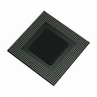
MPC8360EVVAJDGA Freescale Semiconductor, MPC8360EVVAJDGA Datasheet - Page 66

MPC8360EVVAJDGA
Manufacturer Part Number
MPC8360EVVAJDGA
Description
IC MPU POWERQUICC II PRO 740TBGA
Manufacturer
Freescale Semiconductor
Series
PowerQUICC II PROr
Specifications of MPC8360EVVAJDGA
Processor Type
MPC83xx PowerQUICC II Pro 32-Bit
Speed
533MHz
Voltage
1.2V
Mounting Type
Surface Mount
Package / Case
740-TBGA
Processor Series
MPC8xxx
Core
e300
Data Bus Width
32 bit
Development Tools By Supplier
MPC8360E-RDK
Maximum Clock Frequency
533 MHz
Maximum Operating Temperature
+ 105 C
Mounting Style
SMD/SMT
I/o Voltage
1.8 V, 2.5 V, 3.3 V
Minimum Operating Temperature
0 C
Core Size
32 Bit
Program Memory Size
64KB
Cpu Speed
533MHz
Embedded Interface Type
I2C, SPI, USB, UART
Digital Ic Case Style
TBGA
No. Of Pins
740
Rohs Compliant
Yes
For Use With
MPC8360EA-MDS-PB - KIT APPLICATION DEV 8360 SYSTEMMPC8360E-RDK - BOARD REFERENCE DESIGN FOR MPC
Lead Free Status / RoHS Status
Lead free / RoHS Compliant
Features
-
Lead Free Status / Rohs Status
Lead free / RoHS Compliant
Available stocks
Company
Part Number
Manufacturer
Quantity
Price
Company:
Part Number:
MPC8360EVVAJDGA
Manufacturer:
Freescale Semiconductor
Quantity:
135
Company:
Part Number:
MPC8360EVVAJDGA
Manufacturer:
Freescale Semiconductor
Quantity:
10 000
Part Number:
MPC8360EVVAJDGA
Manufacturer:
FREESCALE
Quantity:
20 000
HDLC, BISYNC, Transparent, and Synchronous UART
Figure 49
19.3
Figure 50
specifications generally reference the rising edge of the clock, these AC timing diagrams also apply when
the falling edge is the active edge.
Figure 50
Figure 51
66
MPC8360E/MPC8358E PowerQUICC II Pro Processor Revision 2.x TBGA Silicon Hardware Specifications, Rev. 4
Serial CLK (Output)
Note: The clock edge is selectable.
Serial CLK (Input)
AC Test Load
Note: The clock edge is selectable.
provides the AC test load.
and
shows the timing with external clock.
shows the timing with internal clock.
Output Signals:
Output Signals:
Input Signals:
Input Signals:
Figure 51
(See Note)
(See Note)
(See Note)
(See Note)
Output
represent the AC timing from
t
HEIVKH
Figure 50. AC Timing (External Clock) Diagram
Figure 51. AC Timing (Internal Clock) Diagram
t
HIIVKH
Z
Figure 49. AC Test Load
0
= 50 Ω
t
HEKHOX
t
HIKHOX
t
HIIXKH
t
HEKHOV
tHIKHOV
t
HEIXKH
Table 62
R
and
L
= 50 Ω
Table
63. Note that although the
OV
DD
/2
Freescale Semiconductor


