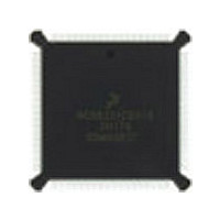
MC68020EH16E Freescale Semiconductor, MC68020EH16E Datasheet - Page 86

MC68020EH16E
Manufacturer Part Number
MC68020EH16E
Description
IC MPU 32BIT 33MHZ 132-PQFP
Manufacturer
Freescale Semiconductor
Datasheet
1.MC68020EH16E.pdf
(306 pages)
Specifications of MC68020EH16E
Processor Type
M680x0 32-Bit
Speed
166MHz
Voltage
5V
Mounting Type
Surface Mount
Package / Case
132-MQFP, 132-PQFP
Family Name
M68000
Device Core
ColdFire
Device Core Size
32b
Frequency (max)
16.67MHz
Instruction Set Architecture
RISC
Supply Voltage 1 (typ)
5V
Operating Supply Voltage (max)
5.25V
Operating Supply Voltage (min)
4.75V
Operating Temp Range
0C to 70C
Operating Temperature Classification
Commercial
Mounting
Surface Mount
Pin Count
132
Package Type
PQFP
Lead Free Status / RoHS Status
Lead free / RoHS Compliant
Features
-
Lead Free Status / Rohs Status
Compliant
Available stocks
Company
Part Number
Manufacturer
Quantity
Price
Company:
Part Number:
MC68020EH16E
Manufacturer:
Freescale Semiconductor
Quantity:
10 000
- Current page: 86 of 306
- Download datasheet (3Mb)
State 4
State 5
5.3.3 Read-Modify-Write Cycle
The read-modify-write cycle performs a read, conditionally modifies the data in the
arithmetic logic unit, and may write the data out to memory. In the MC68020/EC020, this
operation is indivisible, providing semaphore capabilities for multiprocessor systems.
During the entire read-modify-write sequence, the MC68020/EC020 asserts RMC to
indicate that an indivisible operation is occurring. The MC68020/EC020 does not issue a
BG signal in response to a BR signal during this operation.
The TAS, CAS, and CAS2 instructions are the only MC68020/EC020 instructions that
utilize read-modify-write operations. Depending on the compare results of the CAS and
CAS2 instructions, the write cycle(s) may not occur.
Figure 5-29 is a flowchart of the read-modify-write cycle operation. Figure 5-30 is an
example timing diagram of a TAS instruction specified in terms of clock periods.
MOTOROLA
MC68020/EC020—The processor issues no new control signals during S4.
MC68020—The processor negates AS and DS during S5. It holds the address and data
MC68EC020—The processor negates AS and DS during S5. It holds the address and
valid during S5 to provide address hold time for memory systems. R/W , SIZ1, SIZ0,
FC2–FC0, and DBEN also remain valid throughout S5.
The external device must keep DSACK1/DSACK0 asserted until it detects the negation
of AS or DS (whichever it detects first). The device must negate DSACK1/DSACK0
within approximately one clock period after sensing the negation of A S or DS.
DSACK1/DSACK0 signals that remain asserted beyond this limit may be prematurely
detected for the next bus cycle.
data valid during S5 to provide address hold time for memory systems. R/W , SIZ1,
SIZ0, and FC2–FC0 also remain valid throughout S5.
The external device must keep DSACK1/DSACK0 asserted until it detects the negation
of AS or DS (whichever it detects first). The device must negate DSACK1/DSACK0
within approximately one clock period after sensing the negation of A S or DS.
DSACK1/DSACK0 signals that remain asserted beyond this limit may be prematurely
detected for the next bus cycle.
Freescale Semiconductor, Inc.
For More Information On This Product,
Go to: www.freescale.com
M68020 USER’S MANUAL
5- 39
Related parts for MC68020EH16E
Image
Part Number
Description
Manufacturer
Datasheet
Request
R

Part Number:
Description:
(MC600 Series) INTEGRATED CIRCUITS
Manufacturer:
ETC
Datasheet:
Part Number:
Description:
Manufacturer:
Freescale Semiconductor, Inc
Datasheet:
Part Number:
Description:
Manufacturer:
Freescale Semiconductor, Inc
Datasheet:
Part Number:
Description:
Manufacturer:
Freescale Semiconductor, Inc
Datasheet:
Part Number:
Description:
Manufacturer:
Freescale Semiconductor, Inc
Datasheet:
Part Number:
Description:
Manufacturer:
Freescale Semiconductor, Inc
Datasheet:
Part Number:
Description:
Manufacturer:
Freescale Semiconductor, Inc
Datasheet:
Part Number:
Description:
Manufacturer:
Freescale Semiconductor, Inc
Datasheet:
Part Number:
Description:
Manufacturer:
Freescale Semiconductor, Inc
Datasheet:
Part Number:
Description:
Manufacturer:
Freescale Semiconductor, Inc
Datasheet:
Part Number:
Description:
Manufacturer:
Freescale Semiconductor, Inc
Datasheet:
Part Number:
Description:
Manufacturer:
Freescale Semiconductor, Inc
Datasheet:
Part Number:
Description:
Manufacturer:
Freescale Semiconductor, Inc
Datasheet:
Part Number:
Description:
Manufacturer:
Freescale Semiconductor, Inc
Datasheet:
Part Number:
Description:
Manufacturer:
Freescale Semiconductor, Inc
Datasheet:


