MPC8321ECZQAFDC Freescale Semiconductor, MPC8321ECZQAFDC Datasheet - Page 18
MPC8321ECZQAFDC
Manufacturer Part Number
MPC8321ECZQAFDC
Description
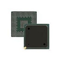
IC MPU PWRQUICC II 516-PBGA
Manufacturer
Freescale Semiconductor
Datasheet
1.MPC8321VRADDC.pdf
(82 pages)
Specifications of MPC8321ECZQAFDC
Processor Type
MPC83xx PowerQUICC II Pro 32-Bit
Speed
333MHz
Voltage
1V
Mounting Type
Surface Mount
Package / Case
516-PBGA
Processor Series
MPC8xxx
Core
e300
Data Bus Width
32 bit
Development Tools By Supplier
MPC8323E-MDS-PB
Maximum Clock Frequency
333 MHz
Maximum Operating Temperature
+ 105 C
Mounting Style
SMD/SMT
Data Ram Size
16 KB
I/o Voltage
1.8 V, 3.3 V
Interface Type
I2C, SPI, UART
Minimum Operating Temperature
- 40 C
Family Name
MPC83xx
Device Core
PowerQUICC II Pro
Device Core Size
32b
Frequency (max)
333MHz
Instruction Set Architecture
RISC
Supply Voltage 1 (typ)
1V
Operating Supply Voltage (max)
1.05V
Operating Supply Voltage (min)
0.95V
Operating Temp Range
-40C to 105C
Operating Temperature Classification
Industrial
Mounting
Surface Mount
Pin Count
516
Package Type
TEBGA
Lead Free Status / RoHS Status
Lead free / RoHS Compliant
Features
-
Lead Free Status / Rohs Status
Lead free / RoHS Compliant
Available stocks
Company
Part Number
Manufacturer
Quantity
Price
Company:

Part Number:
MPC8321ECZQAFDC
Manufacturer:
Freescale Semiconductor
Quantity:
10 000


DDR1 and DDR2 SDRAM
Figure 5
Figure 6
18
MPC8323E PowerQUICC II Pro Integrated Communications Processor Family Hardware Specifications, Rev. 4
ADDR/CMD
MDQS[n]
MDQ[x]
shows the DDR SDRAM output timing for the MCK to MDQS skew measurement (t
shows the DDR1 and DDR2 SDRAM output timing diagram.
MCK[n]
MCK[n]
Figure 6. DDR1 and DDR2 SDRAM Output Timing Diagram
Write A0
t
DDKHMP
MDQS
MDQS
MCK
MCK
Figure 5. Timing Diagram for t
t
DDKHAS
t
DDKHDX
t
MCK
,t
DDKHCS
t
NOOP
DDKHAX
D0
t
DDKHMH
t
DDKHMH
t
MCK
,t
t
DDKHCX
DDKHDS
t
(min) = –0.6 ns
DDKHMH
(max) = 0.6 ns
D1
t
DDKLDS
t
DDKLDX
DDKHMH
Freescale Semiconductor
t
DDKHME
DDKHMH
).
Related parts for MPC8321ECZQAFDC
Image
Part Number
Description
Manufacturer
Datasheet
Request
R

Part Number:
Description:
Mpc8321e Powerquicc Ii Pro Processor
Manufacturer:
Freescale Semiconductor, Inc
Datasheet:
Part Number:
Description:
Manufacturer:
Freescale Semiconductor, Inc
Datasheet:
Part Number:
Description:
Manufacturer:
Freescale Semiconductor, Inc
Datasheet:
Part Number:
Description:
Manufacturer:
Freescale Semiconductor, Inc
Datasheet:
Part Number:
Description:
Manufacturer:
Freescale Semiconductor, Inc
Datasheet:
Part Number:
Description:
Manufacturer:
Freescale Semiconductor, Inc
Datasheet:
Part Number:
Description:
Manufacturer:
Freescale Semiconductor, Inc
Datasheet:
Part Number:
Description:
Manufacturer:
Freescale Semiconductor, Inc
Datasheet:
Part Number:
Description:
Manufacturer:
Freescale Semiconductor, Inc
Datasheet:
Part Number:
Description:
Manufacturer:
Freescale Semiconductor, Inc
Datasheet:
Part Number:
Description:
Manufacturer:
Freescale Semiconductor, Inc
Datasheet:
Part Number:
Description:
Manufacturer:
Freescale Semiconductor, Inc
Datasheet:
Part Number:
Description:
Manufacturer:
Freescale Semiconductor, Inc
Datasheet:
Part Number:
Description:
Manufacturer:
Freescale Semiconductor, Inc
Datasheet:
Part Number:
Description:
Manufacturer:
Freescale Semiconductor, Inc
Datasheet: