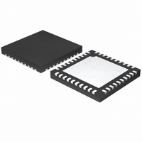
MAX9856ETL+ Maxim Integrated Products, MAX9856ETL+ Datasheet - Page 16

MAX9856ETL+
Manufacturer Part Number
MAX9856ETL+
Description
IC CODEC AUDIO LP 40TQFN-EP
Manufacturer
Maxim Integrated Products
Type
Audio Codecr
Datasheet
1.MAX9856ETL.pdf
(46 pages)
Specifications of MAX9856ETL+
Data Interface
Serial
Resolution (bits)
18 b
Number Of Adcs / Dacs
2 / 2
Sigma Delta
Yes
S/n Ratio, Adcs / Dacs (db) Typ
77 / 91
Dynamic Range, Adcs / Dacs (db) Typ
85 / 91
Voltage - Supply, Analog
1.71 V ~ 3.6 V
Voltage - Supply, Digital
1.71 V ~ 3.6 V
Operating Temperature
-40°C ~ 85°C
Mounting Type
Surface Mount
Package / Case
40-WFQFN Exposed Pad
Number Of Adc Inputs
2
Number Of Dac Outputs
2
Interface Type
I2C
Resolution
18 bit
Operating Supply Voltage
1.71 V to 3.6 V
Maximum Operating Temperature
+ 85 C
Mounting Style
SMD/SMT
Minimum Operating Temperature
- 40 C
Supply Current
2.9 mA
Thd Plus Noise
82 dB
Audio Codec Type
Stereo
No. Of Adcs
2
No. Of Dacs
2
No. Of Input Channels
2
No. Of Output Channels
2
Adc / Dac Resolution
18bit
Adcs / Dacs Signal To Noise Ratio
91dB
Rohs Compliant
Yes
Lead Free Status / RoHS Status
Lead free / RoHS Compliant
Low-Power Audio CODEC with
DirectDrive Headphone Amplifiers
16
PIN
25
26
27
28
29
30
31
32
33
34
35
36
37
38
39
40
—
______________________________________________________________________________________
JACKSNS
LRCLK_A
DVDDS2
MICGND
MICBIAS
SDOUT
NAME
DGND
AGND
MCLK
DVDD
BCLK
MICR
SDIN
INLN
MICL
INLP
EP
Digital Audio Bit Clock Input/Output. BCLK is an input when the MAX9856 is in slave mode and an output
when in master mode.
Digital Audio Serial Data ADC Output
Digital Audio Serial Data DAC Input
Digital Audio Interface I/O Power Supply. Bypass to DGND with 1µF capacitor.
Digital Audio Left-Right Clock Input/Output. LRCLK_A is the audio sample rate clock that determines
whether the audio data on SDOUT is routed to the left or right channel. When only one LRCLK is needed
(ADC and DAC are at the same sample rate), LRCLK_A can be reprogrammed as a general-purpose
input/output, GPIO.
Master Clock Input (CMOS Input). Acceptable Input frequency range: 10MHz to 60MHz.
Digital Power Supply. Supply for the digital core and I
Digital Ground
Inverting Left Differential Input. AC-couple to the low side of microphone, or connect to the negative line
signal. AC-couple to ground when using with a single-ended line or microphone input.
Noninverting Left Differential Input. AC-couple to the high side of microphone, or connect to the positive
line signal. AC-couple to the signal when using with a single-ended line or microphone input.
Left-Channel Single-Ended Microphone Input. AC-couple to the microphone with a 1µF capacitor.
Microphone Ground. Allows the common return signal of a stereo microphone pair to be connected to the
inverting input differential amps in a pseudo differential configuration. Alternatively MICGND can be
grounded for single-ended microphone applications.
Right-Channel Single-Ended Microphone Input. AC-couple to the microphone with a 1µF capacitor.
Low-Noise Bias Voltage. Outputs a 1.5V or 2.4V microphone bias. An external resistor in the 2.2kΩ to 470Ω
range should be used to set the microphone current.
Analog Ground (and Chip Substrate)
Jack Sense. Detects the presence or absence of a jack, and can be configured to detect the impedance
range of the external load. See the Headset Detection section.
Exposed Pad. The exposed pad lowers the package’s thermal impedance by providing a direct heat
conduction path from the die to the PCB. The exposed pad is internally connected to the substrate.
Connect the exposed thermal pad to AGND.
FUNCTION
2
C interface. Bypass to DGND with a 1.0µF capacitor.
Pin Description (continued)


