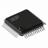
UCB1400BE,151 NXP Semiconductors, UCB1400BE,151 Datasheet - Page 8

UCB1400BE,151
Manufacturer Part Number
UCB1400BE,151
Description
IC AUDIO CODEC 3.3V 48-LQFP
Manufacturer
NXP Semiconductors
Type
Audio Codec '97r
Datasheet
1.UCB1400BEFE.pdf
(63 pages)
Specifications of UCB1400BE,151
Package / Case
48-LQFP
Data Interface
Serial
Resolution (bits)
20 b
Number Of Adcs / Dacs
2 / 2
Sigma Delta
No
S/n Ratio, Adcs / Dacs (db) Typ
97 / 91
Voltage - Supply, Analog
3 V ~ 3.6 V
Voltage - Supply, Digital
3 V ~ 3.6 V
Operating Temperature
-40°C ~ 85°C
Mounting Type
Surface Mount
Mounting Style
SMD/SMT
Lead Free Status / RoHS Status
Lead free / RoHS Compliant
Other names
935269304151
UCB1400BE-SNXP
UCB1400BE-SNXP
UCB1400BE-SNXP
UCB1400BE-SNXP
Available stocks
Company
Part Number
Manufacturer
Quantity
Price
Company:
Part Number:
UCB1400BE,151
Manufacturer:
NXP Semiconductors
Quantity:
10 000
Philips Semiconductors
9397 750 09611
Product data
Fig 6. AC Link audio output frame.
SDATA_OUT
END OF PREVIOUS
BIT_CLK
* See
AUDIO FRAME
SYNC
Table
FRAME
VALID
4.
8.3.2 AC-link audio output frame (SDATA_OUT)
slot(1)
(“1” = TIME SLOT CONTAINS VALID PCM DATA)
TAG PHASE
slot(2)
The audio output frame data streams correspond to the multiplexed bundles of all
digital output data targeting UCB1400’s DAC inputs, and control registers. Each audio
output frame supports up to 12 20-bit outgoing data time slots. Slot 0 is a special
reserved time slot containing 16 bits which are used for AC-link protocol
infrastructure.
Slot 0: TAG:
flags the validity for the entire audio frame. If the ‘Valid Frame’ bit is a 1, this indicates
that the current audio frame contains at least one slot time of valid data. The next 12
bit positions sampled by UCB1400 indicate which of the corresponding 12 time slots
contain valid data. In this way, data streams of differing sample rates can be
transmitted across AC-link at its fixed 48 kHz audio frame rate.
Figure 6
slot 0 tag phase are used for primary/secondary codec addressing as described in
Section
81.4 ns
(12.288 MHz)
A new audio output frame begins with a LOW-to-HIGH transition of SYNC. SYNC is
synchronous to the rising edge of BIT_CLK. On the immediately following falling edge
of BIT_CLK, the UCB1400 samples the assertion of SYNC. This falling edge marks
the time when both sides of AC-link are aware of the start of a new audio frame. On
the next rising of BIT_CLK, the AC ’97 Controller transitions SDATA_OUT into the first
bit position of slot 0 (Valid Frame bit). Each new bit position is presented to AC-link on
a rising edge of BIT_CLK, and subsequently sampled by UCB1400 on the following
falling edge of BIT_CLK. This sequence ensures that data transitions, and
subsequent sample points for both incoming and outgoing data streams are time
aligned.
TIME SLOT “VALID” BITS
slot(12)
8.4.
illustrates the time slot based AC-link protocol. (Note that Bits 1 and 0 of
“0”
Within slot 0, the first bit is a global bit (SDATA_OUT slot 0, bit 15) which
*
Rev. 02 — 21 June 2002
*
(48 kHz)
20.8 s
19
SLOT 1
0
19
Audio codec with touch screen controller
SLOT 2
DATA PHASE
0
and power management monitor
19
© Koninklijke Philips Electronics N.V. 2002. All rights reserved.
SLOT 3
0
UCB1400
19
SLOT 12
SN00221
0
8 of 63


