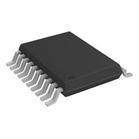
AD5930YRUZ Analog Devices Inc, AD5930YRUZ Datasheet - Page 22

AD5930YRUZ
Manufacturer Part Number
AD5930YRUZ
Description
IC GEN PROG FREQ BURST 20TSSOP
Manufacturer
Analog Devices Inc
Datasheet
1.AD5930YRUZ.pdf
(28 pages)
Specifications of AD5930YRUZ
Resolution (bits)
10 b
Master Fclk
50MHz
Tuning Word Width (bits)
24 b
Voltage - Supply
2.3 V ~ 5.5 V
Operating Temperature
-40°C ~ 125°C
Mounting Type
Surface Mount
Package / Case
20-TSSOP
Synthesizer Type
Frequency
Frequency
25MHz
Supply Voltage Range
2.3V To 5.5V
Supply Current
2.4mA
Operating Temperature Range
-40°C To +105°C
Digital Ic Case Style
TSSOP
No. Of Pins
20
Pin Count
20
Screening Level
Automotive
Package Type
TSSOP
Lead Free Status / RoHS Status
Lead free / RoHS Compliant
Lead Free Status / RoHS Status
Lead free / RoHS Compliant, Lead free / RoHS Compliant
Available stocks
Company
Part Number
Manufacturer
Quantity
Price
Company:
Part Number:
AD5930YRUZ
Manufacturer:
Intel
Quantity:
33
AD5930
APPLICATIONS
GROUNDING AND LAYOUT
The printed circuit board that houses the AD5930 should be
designed so that the analog and digital sections are separated
and confined to certain areas of the board. This facilitates the
use of ground planes that can be easily separated. A minimum
etch technique is generally best for ground planes because it
gives the best shielding. Digital and analog ground planes
should only be joined in one place. If the AD5930 is the only
device requiring an AGND to DGND connection, then the
ground planes should be connected at the AGND and DGND
pins of the AD5930. If the AD5930 is in a system where
multiple devices require AGND to DGND connections, the
connection should be made at one point only, a star ground
point that should be established as close as possible to the
AD5930.
Avoid running digital lines under the device as these couple
noise onto the die. The analog ground plane should be allowed
to run under the AD5930 to avoid noise coupling. The power
supply lines to the AD5930 should use as large a track as
possible to provide low impedance paths and reduce the effects
of glitches on the power supply line. Fast switching signals, such
as clocks, should be shielded with digital ground to avoid
radiating noise to other sections of the board. Avoid crossover
of digital and analog signals. Traces on opposite sides of the
board should run at right angles to each other. This reduces the
effects of feedthrough through the board. A microstrip
technique is by far the best, but is not always possible with a
double-sided board. In this technique, the component side of
the board is dedicated to ground planes, while signals are placed
on the other side.
Good decoupling is important. The analog and digital supplies
to the AD5930 are independent and separately pinned out to
minimize coupling between analog and digital sections of the
device. All analog and digital supplies should be decoupled to
AGND and DGND, respectively, with 0.1 µF ceramic capacitors
in parallel with 10 µF tantalum capacitors. To achieve the best
from the decoupling capacitors, they should be placed as close
as possible to the device, ideally right up against the device. In
systems where a common supply is used to drive both the
AVDD and DVDD of the AD5930, it is recommended that the
system’s AVDD supply be used. This supply should have the
recommended analog supply decoupling between the AVDD
pins of the AD5930 and AGND, and the recommended digital
supply decoupling capacitors between the DVDD pins and
DGND.
Rev. 0 | Page 22 of 28
Proper operation of the comparator requires good layout
strategy. The strategy must minimize the parasitic capacitance
between V
using a ground plane. For example, in a multilayered board, the
V
BIT OUT connected to the bottom layer, so that isolation is
provided between the power and ground planes.
Interfacing to Microprocessors
The AD5930 has a standard serial interface that allows the part
to interface directly with several microprocessors. The device
uses an external serial clock to write the data/control
information into the device. The serial clock can have a
frequency of 40 MHz maximum. The serial clock can be
continuous, or it can idle high or low between write operations.
When data/control information is being written to the AD5930,
FSYNC is taken low and is held low while the 16 bits of data are
being written into the AD5930. The FSYNC signal frames the
16 bits of information being loaded into the AD5930.
AD5930 TO ADSP-21xx INTERFACE
Figure 36 shows the serial interface between the AD5930 and
the ADSP-21xx. The ADSP-21xx should be set up to operate in
the SPORT transmit alternate framing mode (TFSW = 1). The
ADSP-21xx are programmed through the SPORT control
register and should be configured as follows:
1.
2.
3.
4.
5.
Transmission is initiated by writing a word to the Tx register
after the SPORT has been enabled. The data is clocked out on
each rising edge of the serial clock and clocked into the AD5930
on the SCLK falling edge.
IN
signal could be connected to the top layer and the SIGN
Internal clock operation (ISCLK = 1)
Active low framing (INVTFS = 1)
16-bit word length (SLEN = 15)
Internal frame sync signal (ITFS = 1)
Generate a frame sync for each write (TFSR = 1)
Figure 36. ADSP-2101/ADSP-2103 to AD5930 Interface
1
ADDITIONAL PINS OMITTED FOR CLARITY.
IN
ADSP-2103
ADSP-2101/
and the SIGN BIT OUT pin by adding isolation
SCLK
TFS
1
DT
FSYNC
SDATA
SCLK
AD5930
1


