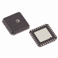
AD9913BCPZ Analog Devices Inc, AD9913BCPZ Datasheet - Page 13

AD9913BCPZ
Manufacturer Part Number
AD9913BCPZ
Description
IC DDS 10BIT DAC 250MSPS 32LFCSP
Manufacturer
Analog Devices Inc
Datasheet
1.AD9913BCPZ.pdf
(32 pages)
Specifications of AD9913BCPZ
Resolution (bits)
10 b
Master Fclk
250MHz
Tuning Word Width (bits)
32 b
Voltage - Supply
1.8 V
Operating Temperature
-40°C ~ 85°C
Mounting Type
Surface Mount
Package / Case
32-LFCSP
Ic Function
Direct Digital Synthesizer
Supply Voltage Range
1.7V To 1.9V
Operating Temperature Range
-40°C To +85°C
Digital Ic Case Style
LFCSP
No. Of Pins
32
Msl
MSL 3 - 168 Hours
Lead Free Status / RoHS Status
Lead free / RoHS Compliant
For Use With
AD9913/PCBZ - BOARD EVAL FOR AD9913
Lead Free Status / RoHS Status
Lead free / RoHS Compliant, Lead free / RoHS Compliant
Available stocks
Company
Part Number
Manufacturer
Quantity
Price
Company:
Part Number:
AD9913BCPZ
Manufacturer:
AD
Quantity:
319
Part Number:
AD9913BCPZ
Manufacturer:
ADI/亚德诺
Quantity:
20 000
AUXILIARY ACCUMULATOR
In addition to the phase accumulator of the DDS, the AD9913
has an auxiliary accumulator. This accumulator can be con-
figured to support either an automatic sweep of one of the
programmable characteristics of the DDS output (frequency or
phase), or it can be configured to implement a change in the
denominator of the frequency equation given in the DDS Core
section. For further details, refer to the Programmable Modulus
Mode section.
10-BIT DAC
The AD9913 incorporates an integrated 10-bit, current output
DAC. The output current is delivered as a balanced signal using
two outputs. The use of balanced outputs reduces the potential
amount of common-mode noise present at the DAC output,
offering the advantage of an increased signal-to-noise ratio. An
external resistor (R
AGND establishes the reference current. The full-scale output
current of the DAC (I
reference current. The recommended value of R
The following equation computes the typical full-scale current
with respect to the R
setting:
The DAC is designed to operate with full-scale current values
up to 4.58 mA. Based on the equation and assuming a 4.62 kΩ
resistor value for R
current for the DAC is 2.28 mA.
Figure 17 shows the range of DAC output current vs. the DAC
FS value assuming an R
I
OUT
(
x
,
R
SET
)
=
SET
SET
set
. 0
, and x = 0x1FF, the nominal output
) connected between the RSET pin and
OUT
R
0206
resistor value and the gain control
SET
SET
) is produced as a scaled version of the
value of 4.62 kΩ.
×
(
1
+
x
)
SET
is 4.62 kΩ.
Rev. A | Page 13 of 32
Pay careful attention to the load termination to ensure that the
output voltage remains within the specified compliance range;
voltages developed beyond this range cause excessive distortion
and can damage the DAC output circuitry.
I/O PORT
The AD9913 I/O port can be configured as a synchronous serial
communications port that allows easy interface to many industry-
standard microcontrollers and microprocessors. The serial I/O port
is compatible with most synchronous transfer formats, including
both the Motorola 6905/11 SPI and Intel 8051 SSR protocols. For
faster programming requirements, a parallel mode is also provided.
PROFILE SELECTIONS
The AD9913 supports the use of profiles, which consist of a group
of eight registers containing pertinent operating parameters for
a particular operating mode. Profiles enable rapid switching
between parameter sets. Profile parameters are programmed via
the I/O port. Once programmed, a specific profile is activated
by means of Register CFR1 Bits [22:20], or three external profile
select pins. The external profile pins option is only available in
serial mode.
5
4
3
2
1
0
0
200
Figure 21. DAC Output Current vs. DAC FS Bits
400
DAC CODE
600
800
1000
1200
AD9913


