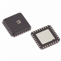
AD9913BCPZ Analog Devices Inc, AD9913BCPZ Datasheet - Page 31

AD9913BCPZ
Manufacturer Part Number
AD9913BCPZ
Description
IC DDS 10BIT DAC 250MSPS 32LFCSP
Manufacturer
Analog Devices Inc
Datasheet
1.AD9913BCPZ.pdf
(32 pages)
Specifications of AD9913BCPZ
Resolution (bits)
10 b
Master Fclk
250MHz
Tuning Word Width (bits)
32 b
Voltage - Supply
1.8 V
Operating Temperature
-40°C ~ 85°C
Mounting Type
Surface Mount
Package / Case
32-LFCSP
Ic Function
Direct Digital Synthesizer
Supply Voltage Range
1.7V To 1.9V
Operating Temperature Range
-40°C To +85°C
Digital Ic Case Style
LFCSP
No. Of Pins
32
Msl
MSL 3 - 168 Hours
Lead Free Status / RoHS Status
Lead free / RoHS Compliant
For Use With
AD9913/PCBZ - BOARD EVAL FOR AD9913
Lead Free Status / RoHS Status
Lead free / RoHS Compliant, Lead free / RoHS Compliant
Available stocks
Company
Part Number
Manufacturer
Quantity
Price
Company:
Part Number:
AD9913BCPZ
Manufacturer:
AD
Quantity:
319
Part Number:
AD9913BCPZ
Manufacturer:
ADI/亚德诺
Quantity:
20 000
Linear Sweep Parameter Register
Address 0x06, 8 bytes are assigned to this register. This register is only effective if CFR1 [11] or CFR1 [28] are set. See the Auxiliary
Accumulator section.
Table 15. Bit Descriptions for Linear Sweep Limit Register
Bit(s)
63:32
31:0
Linear Sweep Delta Parameter Register
Address 0x07, 8 bytes are assigned to this register. This register is only effective if CFR1 [11] or CFR1 [28] are set. See the Auxiliary
Accumulator section.
Table 16. Bit Descriptions for Linear Sweep Step Size Register
Bit(s)
63:32
31:0
Linear Sweep Ramp Rate Register
Address 0x08, 4 bytes are assigned to this register. This register is only effective if CFR1 [11] or CFR1 [28] are set. See the Auxiliary
Accumulator section.
Table 17. Bit Descriptions for Linear Sweep Rate Register
Bit(s)
31:16
15:0
Profile Registers
There are eight consecutive serial I/O addresses dedicated to device profiles. In normal operation, the active profile register is selected
using the external profile select pins.
Profile 0 to Profile 7—Single Tone Register
Address 0x09 to Address 0x10, 6 bytes are assigned to these registers.
Table 18. Bit Descriptions for Profile 0 to Profile 7 Single Tone Register
Bit(s)
47:46
45:32
31:0
Bit Name
Sweep Parameter Word 1
Sweep Parameter Word 0
Bit Name
Falling Delta Word
Rising Delta Word
Bit Name
Falling Sweep Ramp Rate
Rising Sweep Ramp Rate
Bit Name
Open
Phase Offset Word
Frequency Tuning Word
Description
32-bit linear sweep upper limit value. In programmable modulus mode, these bits are used
to set the B value found in the AN-953 Application Note.
32-bit linear sweep lower limit value. In programmable modulus mode, these bits are used
to set the X value found in the AN-953 Application Note.
Description
32-bit linear sweep decrement step size value.
32-bit linear sweep increment step size value. In programmable modulus mode, these bits
are used to set the A value found in the AN-953 Application Note.
Description
16-bit linear sweep negative slope value that defines the time interval between decrement
values.
16-bit linear sweep positive slope value that defines the time interval between increment
values.
Description
Leave these bits at their default state.
This 14-bit number controls the DDS phase offset.
This 32-bit number controls the DDS frequency.
Rev. A | Page 31 of 32
AD9913


