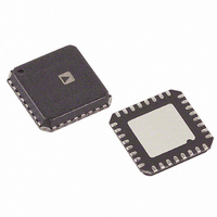
AD9913BCPZ Analog Devices Inc, AD9913BCPZ Datasheet - Page 14

AD9913BCPZ
Manufacturer Part Number
AD9913BCPZ
Description
IC DDS 10BIT DAC 250MSPS 32LFCSP
Manufacturer
Analog Devices Inc
Datasheet
1.AD9913BCPZ.pdf
(32 pages)
Specifications of AD9913BCPZ
Resolution (bits)
10 b
Master Fclk
250MHz
Tuning Word Width (bits)
32 b
Voltage - Supply
1.8 V
Operating Temperature
-40°C ~ 85°C
Mounting Type
Surface Mount
Package / Case
32-LFCSP
Ic Function
Direct Digital Synthesizer
Supply Voltage Range
1.7V To 1.9V
Operating Temperature Range
-40°C To +85°C
Digital Ic Case Style
LFCSP
No. Of Pins
32
Msl
MSL 3 - 168 Hours
Lead Free Status / RoHS Status
Lead free / RoHS Compliant
For Use With
AD9913/PCBZ - BOARD EVAL FOR AD9913
Lead Free Status / RoHS Status
Lead free / RoHS Compliant, Lead free / RoHS Compliant
Available stocks
Company
Part Number
Manufacturer
Quantity
Price
Company:
Part Number:
AD9913BCPZ
Manufacturer:
AD
Quantity:
319
Part Number:
AD9913BCPZ
Manufacturer:
ADI/亚德诺
Quantity:
20 000
AD9913
MODES OF OPERATION
The AD9913 operates in four modes:
•
•
•
•
The modes relate to the data source used to supply the DDS
with its signal control parameters: frequency, phase, or ampli-
tude. The partitioning of the data into different combinations
of frequency, phase, and amplitude is handled automatically
based on the mode and/or specific control bits.
SINGLE TONE MODE
Single tone mode is the default operational mode and is active
when both the direct switch mode bit and the auxiliary
accumulator enable bit are not set. This mode outputs a single
frequency as programmed by the user in the frequency tuning
word (FTW) register. A phase offset value is also available in
single tone mode via the POW register.
DIRECT SWITCH MODE
Direct switch mode enables FSK or PSK modulation. This mode
simply selects the frequency or phase value programmed into
the profile registers. Frequency or phase is determined by the
destination bits in CFR1 [13:12]. Direct switch mode is enabled
using the direct switch mode active bit in register CFR1 [16].
Two approaches are designed for switching between profile
registers. The first is programming the internal profile control
bits, CFR1 [22:20], to the desired value and issuing an
IO_UPDATE. The second approach, with higher data
throughput, is achieved by changing the profile control pins
[2:0]. Control bit CFR1 [27] is for selection between the two
approaches. The default state uses the profile pins.
To perform 8-tone FSK or PSK, program the FTW word or
phase offset word in each profile. The internal profile control
bits or the profile pins are used for the FSK or PSK data.
Table 4 shows the relationship between the profile selection pin
or bit approach.
Table 4. Profile Selection
Profile Pins PS [2:0] or CFR1 Bits [22:20]
000
001
010
011
100
101
110
111
Single tone
Direct switch
Programmable modulus
Linear sweep
Profile Selection
Profile 0
Profile 1
Profile 2
Profile 3
Profile 4
Profile 5
Profile 6
Profile 7
Rev. A | Page 14 of 32
PROGRAMMABLE MODULUS MODE
In programmable modulus mode, the auxiliary accumulator is
used to alter the frequency equation of the DDS core, making it
possible to implement fractions which are not restricted to a
power of 2 in the denominator.
A standard DDS is restricted to powers of 2 as a denominator
because the phase accumulator is a set of bits as wide as the
frequency tuning word. When in programmable modulus
mode, the frequency equation becomes
where 0 ≤ x ≤ 2
When in programmable modulus mode, the auxiliary accumu-
lator is set up to roll over before it reaches full capacity. Every
time it rolls over, an extra LSB value is added to the phase
accumulator. In order to determine the values that must be
programmed in the registers, the user must define the desired
output to sampling clock frequency as a ratio of integers (M/N,
where N must not exceed 2
Refer to the AN-953 Application Note for detailed steps of how
to implement a programmable modulus. The AN-953 defines
how to calculate the three required values (A, B, and X) used for
programmable modulus. The following assigns the required
values to the appropriate register.
•
•
•
LINEAR SWEEP MODE
One purpose of linear sweep mode is to provide better
bandwidth containment compared to direct switch mode by
enabling more gradual, user-defined changes between a starting
point (S0) to an endpoint (E0). The auxiliary accumulator
enable bit is located in Register CFR1 [11]. Linear sweep uses
the auxiliary accumulator to sweep frequency or phase from S0
to E0. A frequency or phase sweep is determined by the
destination bits in CFR1 [13:12]. The trigger to initiate the
sweep can be edge or level triggered. This is determined by
Register CFR1 [9]. Note that, in level triggered mode, the sweep
automatically repeats as long as the appropriate profile pin is
held high.
In linear sweep mode, S0 and E0 (upper and lower limits) are
loaded into the linear sweep parameter register (Register 0x06).
If configured for frequency sweep, the resolution is 32-bits. For
phase sweep, the resolution is 14 bits. When sweeping the
phase, the word value must be MSB-aligned; unused bits are
ignored. The profile pins or the internal profile bits trigger and
control the direction (up/down) of the linear sweep for
frequency or phase. Table 5 depicts the direction of the sweep.
f
f
Register 0x06 [63:32] holds the B value.
Register 0x06 [31:0] holds the X value.
Register 0x07 [31:0] holds the A value.
0
0
= (FTW)(f
= f
S
× (1 − (FTW/x)) with 2
32
.
S
)/x with 0 ≤ FTW ≤ 2
32
).
31
< FTW < 2
31
32
− 1


