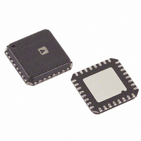
AD9913BCPZ Analog Devices Inc, AD9913BCPZ Datasheet - Page 15

AD9913BCPZ
Manufacturer Part Number
AD9913BCPZ
Description
IC DDS 10BIT DAC 250MSPS 32LFCSP
Manufacturer
Analog Devices Inc
Datasheet
1.AD9913BCPZ.pdf
(32 pages)
Specifications of AD9913BCPZ
Resolution (bits)
10 b
Master Fclk
250MHz
Tuning Word Width (bits)
32 b
Voltage - Supply
1.8 V
Operating Temperature
-40°C ~ 85°C
Mounting Type
Surface Mount
Package / Case
32-LFCSP
Ic Function
Direct Digital Synthesizer
Supply Voltage Range
1.7V To 1.9V
Operating Temperature Range
-40°C To +85°C
Digital Ic Case Style
LFCSP
No. Of Pins
32
Msl
MSL 3 - 168 Hours
Lead Free Status / RoHS Status
Lead free / RoHS Compliant
For Use With
AD9913/PCBZ - BOARD EVAL FOR AD9913
Lead Free Status / RoHS Status
Lead free / RoHS Compliant, Lead free / RoHS Compliant
Available stocks
Company
Part Number
Manufacturer
Quantity
Price
Company:
Part Number:
AD9913BCPZ
Manufacturer:
AD
Quantity:
319
Part Number:
AD9913BCPZ
Manufacturer:
ADI/亚德诺
Quantity:
20 000
Table 5. Determining the Direction of the Linear Sweep
Profile Pins [2:0] or CFR1 Bits [22:20]
x00
x01
x10
x11
1
Note that if the part is used in parallel port programming mode,
the sweep mode is only determined by the internal profile
control bits, CFR1 [22:20]. If the part is used in serial port
programming mode, either the internal profile control bits or
the external profile select pins can work as the sweep control.
CFR1 [27] selects between these two approaches.
Setting the Slope of the Linear Sweep
The slope of the linear sweep is set by the intermediate step size
(delta tuning word) between S0 and E0 (see Figure 22) and the
time spent (sweep ramp rate word) at each step. The resolution
of the delta tuning word is 32 bits for frequency and 14 bits for
phase. The resolution for the delta ramp rate word is 16 bits.
In linear sweep mode, the user programs a rising delta word
(RDW, Register 0x07) and a rising sweep ramp rate (RSRR,
Register 0x08). These settings apply when sweeping from S0 to
E0. The falling delta word (FDW, Register 0x07) and falling
sweep ramp rate (FSRR, Register 0x08) apply when sweeping
from E0 to S0.
Note that if the auxiliary accumulator is allowed to overflow, an
uncontrolled, continuous sweep operation occurs. To avoid this,
the magnitude of the rising or falling delta word should be
smaller than the difference between full-scale and the E0 value
(full-scale − E0). For a frequency sweep, full-scale is 2
a phase sweep, full-scale is 2
Figure 22 displays a linear sweep up and then down. This
depicts the dwell mode (see CRF1 [8]). If the no-dwell bit,
CFR1 [8], is set, the sweep accumulator returns to 0 upon
reaching E0.
x = don’t care.
1
1
1
1
E0
S0
Δf, p
RDW
Figure 22. Linear Sweep Mode
Δt
RSRR
14
− 1.
TIME
FSRR
Linear Sweep Mode
Sweep off
Ramp up
Ramp down
Bidirectional ramp
Δt
FDW
Δf, p
32
− 1. For
Rev. A | Page 15 of 32
For a piecemeal or a nonlinear transition between S0 and E0,
the delta tuning words and ramp rate words can be reprogram-
med during the transition.
The formulas for calculating the step size of RDW or FDW are
The formula for calculating delta time from RSRR or FSRR is
At 250 MSPS operation, (f
interval between steps is 1/250 MHz × 1 = 4 ns. The maximum
time interval is (1/250 MHz) × 65,535= 262 μs.
Frequency Linear Sweep Example
In linear sweep mode, when sweeping from low to high, the
RDW is applied to the input of the auxiliary accumulator and
the RSRR register is loaded into the sweep rate timer.
The RDW accumulates at the rate given by the ramp rate
(RSRR) until the output equals the upper limit in the linear
sweep parameter register (Register 0x06). The sweep is then
complete.
When sweeping from high to low, the FDW is applied to the
input of the auxiliary accumulator and the FSRR register is
loaded into the sweep rate timer.
The FDW accumulates at the rate given by the ramp rate
(FSRR) until the output equals the lower limit in the linear
sweep parameter register value (Register 0x06). The sweep is
then complete. A phase sweep works in the same manner with
fewer bits.
To view sweep capabilities using the profile pins and the no-
dwell bit, refer to Figure 23, Figure 24, and Figure 25.
Frequency
Phase
Phase
Δ
t =
(
Step
Step
RSRR
Step
=
=
)
⎛ π
⎜
⎝
⎛
⎜
⎝
/
45RDW
f
=
SYSCLK
RDW
2
2
⎛
⎜
⎝
13
11
RDW
2
SYSCLK
(Hz)
32
⎞
⎟
⎠
⎞
⎟
⎠
⎞
⎟
⎠
=250 MHz). The minimum time
f
SYSCLK
AD9913
(MHz)
(radians)
(degrees)


