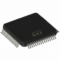
E-STE100P STMicroelectronics, E-STE100P Datasheet - Page 4

E-STE100P
Manufacturer Part Number
E-STE100P
Description
IC TRANSCEIVER 3.3V 64 TQFP
Manufacturer
STMicroelectronics
Type
Transceiverr
Datasheet
1.E-STE100P.pdf
(31 pages)
Specifications of E-STE100P
Number Of Drivers/receivers
1/1
Protocol
MII
Voltage - Supply
3.15 V ~ 3.45 V
Mounting Type
Surface Mount
Package / Case
64-TQFP, 64-VQFP
Number Of Receivers
1
Data Rate
10/100Mbps
Operating Supply Voltage (typ)
3.3V
Package Type
TQFP
Operating Temperature Classification
Industrial
Operating Supply Voltage (max)
3.45V
Operating Supply Voltage (min)
3.15V
Mounting
Surface Mount
Pin Count
64
Operating Temperature (max)
85C
Operating Temperature (min)
-40C
Lead Free Status / RoHS Status
Lead free / RoHS Compliant
Other names
497-2143
STE100P
STE100P
Available stocks
Company
Part Number
Manufacturer
Quantity
Price
Company:
Part Number:
E-STE100P
Manufacturer:
STMicroelectronics
Quantity:
10 000
STE100P
Table 2. Pin Description (continued)
4/31
MII Control Interface
Physical (Twisted Pair) Interface
Pin No.
52
51
43
44
46
47
48
51
49
59
60
42
41
61
12
11
21
23
19
18
Name
rx_clk
rx_dv
mdint
tx_er
rx_er
mdio
rxd4
rxd3
rxd2
rxd1
rxd0
mdc
rxp
rxn
col
crs
txp
txn
x1
x2
Type
OD
I/O
O
O
O
O
O
O
O
O
I
I
I
I
Transmit Coding Error. The MAC asserts this input when an error has occurred
in the transmit data stream. When the STE100P is operating at 100 Mbps, the
STE100P responds by sending invalid code symbols on the line. In Symbol (5B)
Mode this pin functions as txd4.
Receive Data. The STE100P drives received data on these outputs, synchro-
nous to rx_clk.
rxd4 is driven only in Symbol (5B) Mode.
Receive Data Valid. The STE100P asserts This signal when it drives valid data
on rxd. This output is synchronous to rx_clk.
Receive Error. The STE100P asserts this output when it receives invalid sym-
bols from the network. This signal is synchronous to rx_clk. In Symbol (5B) Mode
this pin functions as rxd4.
Receive Clock. This continuous clock provides reference for rxd, rx_dv, and
rx_er signals. Refer to the Clock Requirements discussion in the Functional
Description section.
25 MHz for 100 Mbps operation.
2.5 MHz for 10 Mbps operation.
Collision Detected. The STE100P asserts this output when detecting a collision.
This output remains High for the duration of the collision. This signal is asynchro-
nous and inactive during full-duplex operation.
Carrier Sense. During half-duplex operation (PR0:8=0), the STE100P asserts
this output when either transmit or receive medium is non idle. During full duplex
operation (PR0:8=1), crs is asserted only when the receive medium is non-idle.
Management Data Clock. Clock for the mdio serial data channel. Maximum
frequency is 2.5 MHz.
Management Data Input/Output, Bi-directional serial data channel for PHY
communication.
Management Data Interrupt. When any bit in PR18 = 1, an active High output
on this pin indicates status change in the corresponding bits in PR17.
Interrupt is cleared by reading Register PR17. Requires MDC edge to output.
25 MHz reference clock input. When an external 25 MHz crystal is used, this pin
will be connected to one terminal of it. If an external 25 MHz clock source of
oscillator is used, then this pin will be the input pin of it.
25 MHz reference clock output. When an external 25MHz crystal is used, this pin
will be connected to another terminal of if. If an external clock source is used,
then this pin should be left open.
The differential Transmit outputs of 100Base-TX or 10Base-T, these pins directly
output to the transformer.
The differential Receive inputs of 100Base-TX or 10Base-T, these pins directly
input from the transformer.
Description


