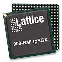
LFE2M70E-6FN900C Lattice, LFE2M70E-6FN900C Datasheet - Page 100

LFE2M70E-6FN900C
Manufacturer Part Number
LFE2M70E-6FN900C
Description
IC, LATTICEECP2M FPGA, 420MHZ, FPBGA-900
Manufacturer
Lattice
Series
LatticeECP2Mr
Datasheet
1.LFE2-12E-5FN256C.pdf
(385 pages)
Specifications of LFE2M70E-6FN900C
No. Of Logic Blocks
67000
No. Of Macrocells
34000
No. Of Speed Grades
6
Total Ram Bits
4534Kbit
No. Of I/o's
416
Clock Management
DLL, PLL
I/o Supply Voltage
3.465V
Rohs Compliant
Yes
Lead Free Status / Rohs Status
Lead free / RoHS Compliant
Available stocks
Company
Part Number
Manufacturer
Quantity
Price
Company:
Part Number:
LFE2M70E-6FN900C
Manufacturer:
LATTICE
Quantity:
47
Company:
Part Number:
LFE2M70E-6FN900C
Manufacturer:
Lattice Semiconductor Corporation
Quantity:
10 000
- Current page: 100 of 385
- Download datasheet (3Mb)
Lattice Semiconductor
Switching Test Conditions
Figure 3-23 shows the output test load that is used for AC testing. The specific values for resistance, capacitance,
voltage, and other test conditions are shown in Table 3-18.
Figure 3-22. Output Test Load, LVTTL and LVCMOS Standards
Table 3-18. Test Fixture Required Components, Non-Terminated Interfaces
LVTTL and other LVCMOS settings (L -> H, H -> L)
LVCMOS 2.5 I/O (Z -> H)
LVCMOS 2.5 I/O (Z -> L)
LVCMOS 2.5 I/O (H -> Z)
LVCMOS 2.5 I/O (L -> Z)
Note: Output test conditions for all other interfaces are determined by the respective standards.
Test Condition
*CL Includes Test Fixture and Probe Capacitance
DUT
V
R1
R2
T
1MΩ
100
R
∞
∞
∞
1
3-49
1MΩ
100
R
∞
∞
∞
CL*
2
Test Poi nt
0pF
C
DC and Switching Characteristics
LatticeECP2/M Family Data Sheet
L
LVCMOS 3.3 = 1.5V
LVCMOS 2.5 = V
LVCMOS 1.8 = V
LVCMOS 1.5 = V
LVCMOS 1.2 = V
V
V
V
V
OH
OL
CCIO
CCIO
+ 0.10
- 0.10
/2
/2
Timing Ref.
CCIO
CCIO
CCIO
CCIO
/2
/2
/2
/2
V
V
CCIO
CCIO
V
—
—
—
—
—
—
—
T
Related parts for LFE2M70E-6FN900C
Image
Part Number
Description
Manufacturer
Datasheet
Request
R
Part Number:
Description:
Manufacturer:
Lattice Semiconductor Corp.
Datasheet:
Part Number:
Description:
IC, LATTICEECP2M FPGA, 420MHZ, FPBGA-900
Manufacturer:
LATTICE SEMICONDUCTOR
Datasheet:

Part Number:
Description:
IC FPGA 50KLUTS 410I/O 900-BGA
Manufacturer:
Lattice
Datasheet:

Part Number:
Description:
IC FPGA 50KLUTS 410I/O 900-BGA
Manufacturer:
Lattice
Datasheet:

Part Number:
Description:
IC FPGA 67KLUTS 1152FPBGA
Manufacturer:
Lattice
Datasheet:

Part Number:
Description:
IC FPGA 67KLUTS 900FPBGA
Manufacturer:
Lattice
Datasheet:

Part Number:
Description:
IC FPGA 67KLUTS 1152FPBGA
Manufacturer:
Lattice
Datasheet:

Part Number:
Description:
IC FPGA 67KLUTS 1152FPBGA
Manufacturer:
Lattice
Datasheet:

Part Number:
Description:
IC FPGA 67KLUTS 1152FPBGA
Manufacturer:
Lattice
Datasheet:

Part Number:
Description:
FPGA - Field Programmable Gate Array 67K LUTs 430 I/O Memry DSP 1.2V -5Spd
Manufacturer:
Lattice

Part Number:
Description:
FPGA - Field Programmable Gate Array 67K LUTs 430 I/O Memry DSP 1.2V -7Spd
Manufacturer:
Lattice

Part Number:
Description:
FPGA - Field Programmable Gate Array 67K LUTs 430 I/O Memry DSP 1.2V -5Spd
Manufacturer:
Lattice

Part Number:
Description:
FPGA - Field Programmable Gate Array 67K LUTs 430 I/O Memry DSP 1.2V -6Spd
Manufacturer:
Lattice

Part Number:
Description:
FPGA - Field Programmable Gate Array 67K LUTs 416 I/O Memory DSP 1.2V 5SPD
Manufacturer:
Lattice


