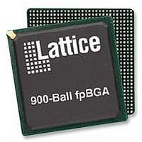
LFE2M70E-6FN900C Lattice, LFE2M70E-6FN900C Datasheet - Page 138

LFE2M70E-6FN900C
Manufacturer Part Number
LFE2M70E-6FN900C
Description
IC, LATTICEECP2M FPGA, 420MHZ, FPBGA-900
Manufacturer
Lattice
Series
LatticeECP2Mr
Datasheet
1.LFE2-12E-5FN256C.pdf
(385 pages)
Specifications of LFE2M70E-6FN900C
No. Of Logic Blocks
67000
No. Of Macrocells
34000
No. Of Speed Grades
6
Total Ram Bits
4534Kbit
No. Of I/o's
416
Clock Management
DLL, PLL
I/o Supply Voltage
3.465V
Rohs Compliant
Yes
Lead Free Status / Rohs Status
Lead free / RoHS Compliant
Available stocks
Company
Part Number
Manufacturer
Quantity
Price
Company:
Part Number:
LFE2M70E-6FN900C
Manufacturer:
LATTICE
Quantity:
47
Company:
Part Number:
LFE2M70E-6FN900C
Manufacturer:
Lattice Semiconductor Corporation
Quantity:
10 000
- Current page: 138 of 385
- Download datasheet (3Mb)
Lattice Semiconductor
LFE2-6E/SE and LFE2-12E/SE Logic Signal Connections: 256 fpBGA (Cont.)
Number
* Supports true LVDS. Other differential signals must be emulated with external resistors.
** These dedicated input pins can be used for GPLLs or GDLLs within the respective quadrant.
Note: VCCIO and GND pads are used to determine the average DC current drawn by I/Os between GND/VCCIO connections, or between the
last GND/VCCIO in an I/O bank and the end of an I/O bank. The substrate pads listed in the Pin Table do not necessarily have a one to one
connection with a package ball or pin.
Ball
R12
T16
R5
T1
Function
Ball/Pad
GND
GND
GND
GND
Bank
LFE2-6E/SE
-
-
-
-
Dual Function
Differential
4-38
Function
Ball/Pad
GND
GND
GND
GND
LatticeECP2/M Family Data Sheet
Bank
-
-
-
-
LFE2-12E/SE
Dual Function
Pinout Information
Differential
Related parts for LFE2M70E-6FN900C
Image
Part Number
Description
Manufacturer
Datasheet
Request
R
Part Number:
Description:
Manufacturer:
Lattice Semiconductor Corp.
Datasheet:
Part Number:
Description:
IC, LATTICEECP2M FPGA, 420MHZ, FPBGA-900
Manufacturer:
LATTICE SEMICONDUCTOR
Datasheet:

Part Number:
Description:
IC FPGA 50KLUTS 410I/O 900-BGA
Manufacturer:
Lattice
Datasheet:

Part Number:
Description:
IC FPGA 50KLUTS 410I/O 900-BGA
Manufacturer:
Lattice
Datasheet:

Part Number:
Description:
IC FPGA 67KLUTS 1152FPBGA
Manufacturer:
Lattice
Datasheet:

Part Number:
Description:
IC FPGA 67KLUTS 900FPBGA
Manufacturer:
Lattice
Datasheet:

Part Number:
Description:
IC FPGA 67KLUTS 1152FPBGA
Manufacturer:
Lattice
Datasheet:

Part Number:
Description:
IC FPGA 67KLUTS 1152FPBGA
Manufacturer:
Lattice
Datasheet:

Part Number:
Description:
IC FPGA 67KLUTS 1152FPBGA
Manufacturer:
Lattice
Datasheet:

Part Number:
Description:
FPGA - Field Programmable Gate Array 67K LUTs 430 I/O Memry DSP 1.2V -5Spd
Manufacturer:
Lattice

Part Number:
Description:
FPGA - Field Programmable Gate Array 67K LUTs 430 I/O Memry DSP 1.2V -7Spd
Manufacturer:
Lattice

Part Number:
Description:
FPGA - Field Programmable Gate Array 67K LUTs 430 I/O Memry DSP 1.2V -5Spd
Manufacturer:
Lattice

Part Number:
Description:
FPGA - Field Programmable Gate Array 67K LUTs 430 I/O Memry DSP 1.2V -6Spd
Manufacturer:
Lattice

Part Number:
Description:
FPGA - Field Programmable Gate Array 67K LUTs 416 I/O Memory DSP 1.2V 5SPD
Manufacturer:
Lattice


