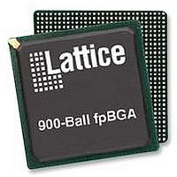
LFE2M70E-6FN900C Lattice, LFE2M70E-6FN900C Datasheet - Page 21

LFE2M70E-6FN900C
Manufacturer Part Number
LFE2M70E-6FN900C
Description
IC, LATTICEECP2M FPGA, 420MHZ, FPBGA-900
Manufacturer
Lattice
Series
LatticeECP2Mr
Datasheet
1.LFE2-12E-5FN256C.pdf
(385 pages)
Specifications of LFE2M70E-6FN900C
No. Of Logic Blocks
67000
No. Of Macrocells
34000
No. Of Speed Grades
6
Total Ram Bits
4534Kbit
No. Of I/o's
416
Clock Management
DLL, PLL
I/o Supply Voltage
3.465V
Rohs Compliant
Yes
Lead Free Status / Rohs Status
Lead free / RoHS Compliant
Available stocks
Company
Part Number
Manufacturer
Quantity
Price
Company:
Part Number:
LFE2M70E-6FN900C
Manufacturer:
LATTICE
Quantity:
47
Company:
Part Number:
LFE2M70E-6FN900C
Manufacturer:
Lattice Semiconductor Corporation
Quantity:
10 000
- Current page: 21 of 385
- Download datasheet (3Mb)
Lattice Semiconductor
Figure 2-19. Edge Clock Mux Connections
sysMEM Memory
LatticeECP2/M devices contains a number of sysMEM Embedded Block RAM (EBR). The EBR consists of an 18-
Kbit RAM with dedicated input and output registers.
sysMEM Memory Block
The sysMEM block can implement single port, dual port or pseudo dual port memories. Each block can be used in
a variety of depths and widths as shown in Table 2-6. FIFOs can be implemented in sysMEM EBR blocks by imple-
menting support logic with PFUs. The EBR block facilitates parity checking by supporting an optional parity bit for
each data byte. EBR blocks provide byte-enable support for configurations with18-bit and 36-bit data widths.
GPLL Output CLKOP
GPLL Output CLKOS
DLL Output CLKOP
DLL Output CLKOS
Clock Input Pad
GPLL Input Pad
GPLL Input Pad
Input Pad
Input Pad
Routing
Routing
Routing
CLKO
CLKO
2-18
Top and Bottom
ECLK1/ ECLK2
Left and Right
Left and Right
Edge Clocks
Edge Clocks
Edge Clocks
(Both Mux)
LatticeECP2/M Family Data Sheet
ECLK1
ECLK2
Architecture
Related parts for LFE2M70E-6FN900C
Image
Part Number
Description
Manufacturer
Datasheet
Request
R
Part Number:
Description:
Manufacturer:
Lattice Semiconductor Corp.
Datasheet:
Part Number:
Description:
IC, LATTICEECP2M FPGA, 420MHZ, FPBGA-900
Manufacturer:
LATTICE SEMICONDUCTOR
Datasheet:

Part Number:
Description:
IC FPGA 50KLUTS 410I/O 900-BGA
Manufacturer:
Lattice
Datasheet:

Part Number:
Description:
IC FPGA 50KLUTS 410I/O 900-BGA
Manufacturer:
Lattice
Datasheet:

Part Number:
Description:
IC FPGA 67KLUTS 1152FPBGA
Manufacturer:
Lattice
Datasheet:

Part Number:
Description:
IC FPGA 67KLUTS 900FPBGA
Manufacturer:
Lattice
Datasheet:

Part Number:
Description:
IC FPGA 67KLUTS 1152FPBGA
Manufacturer:
Lattice
Datasheet:

Part Number:
Description:
IC FPGA 67KLUTS 1152FPBGA
Manufacturer:
Lattice
Datasheet:

Part Number:
Description:
IC FPGA 67KLUTS 1152FPBGA
Manufacturer:
Lattice
Datasheet:

Part Number:
Description:
FPGA - Field Programmable Gate Array 67K LUTs 430 I/O Memry DSP 1.2V -5Spd
Manufacturer:
Lattice

Part Number:
Description:
FPGA - Field Programmable Gate Array 67K LUTs 430 I/O Memry DSP 1.2V -7Spd
Manufacturer:
Lattice

Part Number:
Description:
FPGA - Field Programmable Gate Array 67K LUTs 430 I/O Memry DSP 1.2V -5Spd
Manufacturer:
Lattice

Part Number:
Description:
FPGA - Field Programmable Gate Array 67K LUTs 430 I/O Memry DSP 1.2V -6Spd
Manufacturer:
Lattice

Part Number:
Description:
FPGA - Field Programmable Gate Array 67K LUTs 416 I/O Memory DSP 1.2V 5SPD
Manufacturer:
Lattice


