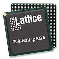
LFE2M70E-6FN900C Lattice, LFE2M70E-6FN900C Datasheet - Page 23

LFE2M70E-6FN900C
Manufacturer Part Number
LFE2M70E-6FN900C
Description
IC, LATTICEECP2M FPGA, 420MHZ, FPBGA-900
Manufacturer
Lattice
Series
LatticeECP2Mr
Datasheet
1.LFE2-12E-5FN256C.pdf
(385 pages)
Specifications of LFE2M70E-6FN900C
No. Of Logic Blocks
67000
No. Of Macrocells
34000
No. Of Speed Grades
6
Total Ram Bits
4534Kbit
No. Of I/o's
416
Clock Management
DLL, PLL
I/o Supply Voltage
3.465V
Rohs Compliant
Yes
Lead Free Status / Rohs Status
Lead free / RoHS Compliant
Available stocks
Company
Part Number
Manufacturer
Quantity
Price
Company:
Part Number:
LFE2M70E-6FN900C
Manufacturer:
LATTICE
Quantity:
47
Company:
Part Number:
LFE2M70E-6FN900C
Manufacturer:
Lattice Semiconductor Corporation
Quantity:
10 000
- Current page: 23 of 385
- Download datasheet (3Mb)
Lattice Semiconductor
Figure 2-20. Memory Core Reset
For further information about the sysMEM EBR block, please see the the list of additional technical documentation
at the end of this data sheet.
EBR Asynchronous Reset
EBR asynchronous reset or GSR (if used) can only be applied if all clock enables are low for a clock cycle before the
reset is applied and released a clock cycle after the reset is released, as shown in Figure 2-21. The GSR input to the
EBR is always asynchronous.
Figure 2-21. EBR Asynchronous Reset (Including GSR) Timing Diagram
If all clock enables remain enabled, the EBR asynchronous reset or GSR may only be applied and released after
the EBR read and write clock inputs are in a steady state condition for a minimum of 1/f
release must adhere to the EBR synchronous reset setup time before the next active read or write clock edge.
If an EBR is pre-loaded during configuration, the GSR input must be disabled or the release of the GSR during
device Wake Up must occur before the release of the device I/Os becomes active.
These instructions apply to all EBR RAM and ROM implementations.
Note that there are no reset restrictions if the EBR synchronous reset is used and the EBR GSR input is disabled.
sysDSP™ Block
The LatticeECP2/M family provides a sysDSP block, making it ideally suited for low cost, high performance Digital
Signal Processing (DSP) applications. Typical functions used in these applications are Finite Impulse Response
GSRN
RSTA
RSTB
Programmable Disable
Reset
Clock
Clock
Enable
Memory Core
2-20
Output Data
L
L
D
D
Latches
CLR
CLR
SET
SET
Q
Q
LatticeECP2/M Family Data Sheet
Port A[17:0]
Port B[17:0]
MAX
(EBR clock). The reset
Architecture
Related parts for LFE2M70E-6FN900C
Image
Part Number
Description
Manufacturer
Datasheet
Request
R
Part Number:
Description:
Manufacturer:
Lattice Semiconductor Corp.
Datasheet:
Part Number:
Description:
IC, LATTICEECP2M FPGA, 420MHZ, FPBGA-900
Manufacturer:
LATTICE SEMICONDUCTOR
Datasheet:

Part Number:
Description:
IC FPGA 50KLUTS 410I/O 900-BGA
Manufacturer:
Lattice
Datasheet:

Part Number:
Description:
IC FPGA 50KLUTS 410I/O 900-BGA
Manufacturer:
Lattice
Datasheet:

Part Number:
Description:
IC FPGA 67KLUTS 1152FPBGA
Manufacturer:
Lattice
Datasheet:

Part Number:
Description:
IC FPGA 67KLUTS 900FPBGA
Manufacturer:
Lattice
Datasheet:

Part Number:
Description:
IC FPGA 67KLUTS 1152FPBGA
Manufacturer:
Lattice
Datasheet:

Part Number:
Description:
IC FPGA 67KLUTS 1152FPBGA
Manufacturer:
Lattice
Datasheet:

Part Number:
Description:
IC FPGA 67KLUTS 1152FPBGA
Manufacturer:
Lattice
Datasheet:

Part Number:
Description:
FPGA - Field Programmable Gate Array 67K LUTs 430 I/O Memry DSP 1.2V -5Spd
Manufacturer:
Lattice

Part Number:
Description:
FPGA - Field Programmable Gate Array 67K LUTs 430 I/O Memry DSP 1.2V -7Spd
Manufacturer:
Lattice

Part Number:
Description:
FPGA - Field Programmable Gate Array 67K LUTs 430 I/O Memry DSP 1.2V -5Spd
Manufacturer:
Lattice

Part Number:
Description:
FPGA - Field Programmable Gate Array 67K LUTs 430 I/O Memry DSP 1.2V -6Spd
Manufacturer:
Lattice

Part Number:
Description:
FPGA - Field Programmable Gate Array 67K LUTs 416 I/O Memory DSP 1.2V 5SPD
Manufacturer:
Lattice


