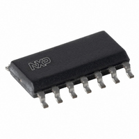
AU5783D,512 NXP Semiconductors, AU5783D,512 Datasheet - Page 10

AU5783D,512
Manufacturer Part Number
AU5783D,512
Description
IC TRANSCEIVER VPW 14-SOIC
Manufacturer
NXP Semiconductors
Series
AUr
Type
Transceiverr
Datasheet
1.AU5783D512.pdf
(14 pages)
Specifications of AU5783D,512
Number Of Drivers/receivers
1/1
Protocol
J1850
Voltage - Supply
5.5 V ~ 16 V
Mounting Type
Surface Mount
Package / Case
14-SOIC (3.9mm Width), 14-SOL
Lead Free Status / RoHS Status
Lead free / RoHS Compliant
Other names
568-3052-5
935263974512
AU5783D
935263974512
AU5783D
1. This parameter is characterized but not subject to production test.
Philips Semiconductors
DYNAMIC CHARACTERISTICS
7 V < V
BUS: 250
Bus load A: R
R/F pin: R
RX pin: R
Typical values reflect the approximate average value at V
NSTB and 4X/LOOP rise and fall times < 10 ns.
NOTES:
2001 Feb 15
INH output function
BUS output function
BUS input function
SYMBOL
J1850/VPW transceiver with supply control function
CTX
t
t
t
t
t
t
t
t
t
t
t
t
B
t
t
t
t
t
t
t
t
t
t
t
inhoff
inhonl
inhonr
BOon
BOoff
BrA
BrB
BfA
BfB
ir
if
wBh
BO4Xon
BO4Xoff
pon
poff
plbon
plboff
DRXon
DRXoff
tRX
tRXsl
DRXsl
HRM
;
BAT
;
;
;
;
d
< 16 V; –40 C < T
s
= 3.9 k to 5 V; C
= 56 k
TX input capacitance
INH turn-off delay
LWAKE to INH turn-on delay
BUS to INH turn-on delay
Delay TX to BUS rising and
falling edge
BUS voltage rise time
BUS voltage rise time
BUS output voltage fall time
BUS output voltage fall time
BUS output current rise time
BUS output current fall time
BUS high pulse width
BUS output voltage harmonic
content; normal mode
TX to BUS delay in 4X mode
Delay TX to RX rising and
falling edge in normal mode
Delay TX to RX rising and
falling edge in loop-back mode
BUS input delay time, rising
and falling edge
RX output transition time, rising
and falling edge
RX output transition time in
standby and sleep mode, rising
and falling edge
BUS to RX delay in sleep and
standby modes
< R
L
= 1.38 k , C
L
< 1.6 k ; 3 nF < C
PARAMETER
1%; INH loaded with 100 k and 30 pF to GND
amb
L
L
= 3.3 nF; Bus load B: R
= 30 pF to GND; NSTB = 5 V; 4X/LOOP = 0 V
< +125 C; –2 V < V
L
< 17 nF; 1.7 s < (R
Note 1
BUS = 0 V, LWAKE = V
measured from NSTB = 0.9 V to INH = 3.5 V
NSTB = 0 V, BUS = 0 V, measured from LWAKE = 3 V to
INH = 3.5 V
sleep mode, LWAKE = V
INH = 3.5 V
from TX = 2.5 V to BUS = 3.875 V; bus load A and bus load B
bus load A, 9 V < V
bus load B, 9 V < V
bus load A, 9 V < V
bus load B, 9 V < V
bus load B connected to –2 V,
9 V < V
capacitor current
bus load B connected to –2 V,
9 V < V
capacitor current
TX = high for 64 s, bus load condition A, 9 V < V
minimum width measured at BUS = 6.25 V, maximum width
measured at BUS = 1.5 V
f = 530 kHz to 1670 kHz, bus load B connected to –2 V,
TX = 7.81 kHz, 50% duty cycle, 9 V < V
4X/LOOP = 1 V, bus load B,
9 V < V
measured from 1.8 V on TX to 2.5 V on RX
NSTB = 5 V, 4X = floating, measured from 1.8 V on TX to
2.5 V on RX
measured from V
NSTB = 5 V, measured at 10% and 90% of waveform
NSTB = 0 V, measured at 10% and 90% of waveform
NSTB = 0 V, LWAKE = V
to RX = 2.5 V
bus
BAT
BAT
BAT
L
BAT
< +9 V; 1.4 k < R
= 300 , C
< 16 V, measured at 20% and 80% of load
< 16 V, measured at 20% and 80% of load
< 16 V, from TX = 1.8 V to BUS = 3.875 V
L
= 13 V and T
* C
L
BUS
) < 5.2 s
BAT
BAT
BAT
BAT
L
= 3.875 V to V
= 16.5 nF
10
CONDITIONS
BAT
< 16 V, measured at 1.5 V and 6.25 V
< 16 V, measured at 1.5 V and 6.25 V
< 16 V, measured at 1.5 V and 6.25 V
< 16 V, measured at 1.5 V and 6.25 V
BAT
BAT
amb
, measured from BUS = 3.875 V to
or 0 V, go to sleep command,
, measured from BUS = 3.875 V
ld
< 12 k
= 25 C, unless otherwise specified.
RX
= 2.5 V
BAT
< 16 V, Note 1
BAT
< 16 V;
13
11
11
11
11
4
4
35
0.5
13
13
0.2
8
MIN.
Preliminary specification
TYP.
AU5783
15
200
100
60
22
18
18
18
18
93
70
5
25
25
2
1
5
60
MAX.
pF
dB V
UNIT
s
s
s
s
s
s
s
s
s
s
s
s
s
s
s
s
s
s


