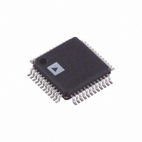
ADV7173KST Analog Devices Inc, ADV7173KST Datasheet - Page 24

ADV7173KST
Manufacturer Part Number
ADV7173KST
Description
IC DAC VIDEO NTSC 6-CH 48LQFP
Manufacturer
Analog Devices Inc
Type
Video Encoderr
Datasheet
1.ADV7173KSTZ.pdf
(60 pages)
Specifications of ADV7173KST
Rohs Status
RoHS non-compliant
Applications
Multimedia
Voltage - Supply, Analog
4.75 V ~ 5.25 V
Mounting Type
Surface Mount
Package / Case
48-LQFP
Number Of Dac's
6
Adc/dac Resolution
10b
Screening Level
Commercial
Package Type
LQFP
Pin Count
48
For Use With
EVAL-ADV7173EBM - BOARD EVAL FOR ADV7173
Voltage - Supply, Digital
-
Lead Free Status / RoHS Status
Not Compliant
Available stocks
Company
Part Number
Manufacturer
Quantity
Price
Company:
Part Number:
ADV7173KST
Manufacturer:
AD
Quantity:
1 831
Company:
Part Number:
ADV7173KST-REEL
Manufacturer:
AD
Quantity:
1
Company:
Part Number:
ADV7173KSTZ
Manufacturer:
ADI
Quantity:
1 135
Company:
Part Number:
ADV7173KSTZ
Manufacturer:
Analog Devices Inc
Quantity:
10 000
Part Number:
ADV7173KSTZ
Manufacturer:
ADI/亚德诺
Quantity:
20 000
Company:
Part Number:
ADV7173KSTZ-REEL
Manufacturer:
ADI
Quantity:
7 101
Company:
Part Number:
ADV7173KSTZ-REEL
Manufacturer:
Analog Devices Inc
Quantity:
10 000
ADV7172/ADV7173
CSO, HSO, AND VSO OUTPUTS
The ADV7172/ADV7173 supports three timing signals, CSO
(composite sync signal), HSO (horizontal sync signal) and VSO
(vertical sync signal). These output TTL signals are aligned with
the analog video outputs. HSO and CSO are shared on Pin 10.
Mode Register 7, Bit MR75 can be used to configure this out-
put pin. See Figure 37 for an example of these waveforms.
CLAMP OUTPUT
The ADV7172/ADV7173 has a programmable clamp TTL
output signal. The clamp signal is programmable to the front
and back porch. Mode Register 5, Bit MR57 can be used to
control the porch position. Also the position of the clamp signal
can be varied by 1–3 clock cycles in a positive and negative
direction from the default position. Mode Register 5, Bits MR56,
MR55, and MR54 control this position.
MPU PORT DESCRIPTION
The ADV7172 and ADV7173 support a 2-wire serial (I
Compatible) microprocessor bus driving multiple peripherals.
Two inputs serial data (SDATA) and serial clock (SCLOCK)
carry information between any device connected to the bus.
Each slave device is recognized by a unique address. The
ADV7172 and ADV7173 each have four possible slave addresses
for both read and write operations. These are unique addresses
for each device and are illustrated in Figure 39 and Figure 40.
The LSB sets either a read or write operation. Logic Level
“1” corresponds to a read operation while Logic Level “0”
corresponds to a write operation. A1 is set by setting the ALSB
pin of the ADV7172/ADV7173 to Logic Level “0” or Logic
Level “1.” When ALSB is set to “0,” there is greater bandwidth
on the I
bus. When ALSB is set to “1,” there is reduced input band-
MR57 = 0
MR57 = 1
2
C lines, which allows high-speed data transfers on this
0H
EXAMPLE: NTSC
OUTPUT
VIDEO
CSO
HSO
VSO
525
1
2
3
CSO HSO VSO
2
C-
4
5
width on the I
than 50 ns will not pass into the I
mode is recommended for noisy systems.
To control the various devices on the bus the following protocol
must be followed. First the master initiates a data transfer by
establishing a start condition, defined by a high-to-low transition
on SDATA while SCLOCK remains high. This indicates that
an address/data stream will follow. All peripherals respond to
the Start condition and shift the next eight bits (7-bit address +
R/W bit). The bits are transferred from MSB down to LSB. The
peripheral that recognizes the transmitted address responds by
pulling the data line low during the ninth clock pulse. This is
known as an acknowledge bit. All other devices withdraw from
the bus at this point and maintain an idle condition. The idle
condition is where the device monitors the SDATA and SCLOCK
lines waiting for the Start condition and the correct transmitted
address. The R/W bit determines the direction of the data. A
Logic “0” on the LSB of the first byte means that the master
will write information to the peripheral. A Logic “1” on the LSB
of the first byte means that the master will read information
from the peripheral.
6
1
0
7
2
1
1
C lines, which means that impulses of less
0
0
8
1
1
9
0
0
2
C internal controller. This
10
1
1
SET UP BY
SET UP BY
ADDRESS
CONTROL
ADDRESS
CONTROL
ALSB
ALSB
11-19
A1
A1
READ/WRITE
READ/WRITE
0
1
0
1
CONTROL
CONTROL
X
X
WRITE
READ
WRITE
READ


