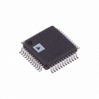
ADV7173KST Analog Devices Inc, ADV7173KST Datasheet - Page 37

ADV7173KST
Manufacturer Part Number
ADV7173KST
Description
IC DAC VIDEO NTSC 6-CH 48LQFP
Manufacturer
Analog Devices Inc
Type
Video Encoderr
Datasheet
1.ADV7173KSTZ.pdf
(60 pages)
Specifications of ADV7173KST
Rohs Status
RoHS non-compliant
Applications
Multimedia
Voltage - Supply, Analog
4.75 V ~ 5.25 V
Mounting Type
Surface Mount
Package / Case
48-LQFP
Number Of Dac's
6
Adc/dac Resolution
10b
Screening Level
Commercial
Package Type
LQFP
Pin Count
48
For Use With
EVAL-ADV7173EBM - BOARD EVAL FOR ADV7173
Voltage - Supply, Digital
-
Lead Free Status / RoHS Status
Not Compliant
Available stocks
Company
Part Number
Manufacturer
Quantity
Price
Company:
Part Number:
ADV7173KST
Manufacturer:
AD
Quantity:
1 831
Company:
Part Number:
ADV7173KST-REEL
Manufacturer:
AD
Quantity:
1
Company:
Part Number:
ADV7173KSTZ
Manufacturer:
ADI
Quantity:
1 135
Company:
Part Number:
ADV7173KSTZ
Manufacturer:
Analog Devices Inc
Quantity:
10 000
Part Number:
ADV7173KSTZ
Manufacturer:
ADI/亚德诺
Quantity:
20 000
Company:
Part Number:
ADV7173KSTZ-REEL
Manufacturer:
ADI
Quantity:
7 101
Company:
Part Number:
ADV7173KSTZ-REEL
Manufacturer:
Analog Devices Inc
Quantity:
10 000
TELETEXT REQUEST CONTROL REGISTER TC07
(TC07–TC00)
(Address (SR4–SR0) = 1CH)
Teletext Control Register is an 8-bit-wide register. See Figure 59.
TTXREQ Rising Edge Control (TC07–TC04)
These bits control the position of the rising edge of TTXREQ.
It can be programmed from zero CLOCK cycles to a max of 15
CLOCK cycles.
TTXREQ Falling Edge Control (TC03–TC00)
These bits control the position of the falling edge of TTXREQ.
It can be programmed from zero CLOCK cycles to a max of 15
CLOCK cycles. This controls the active window for Teletext
data. Increasing this value reduces the amount of Teletext Bits
below the default of 360. If Bits TC03–TC00 are 00Hex when
Bits TC07–TC04 are changed, then the falling edge of TTXREQ
will track that of the rising edge (i.e., the time between the fall-
ing and rising edge remains constant).
CGMS_WSS REGISTER 0 C/W0 (C/W07–C/W00)
(Address (SR4–SR0) = 19H)
CGMS_WSS Register 0 is an 8-bit-wide register. Figure 60
shows the operations under control of this register.
C/W07
WIDE SCREEN SIGNAL
0
1
CONTROL
TC07
DISABLE
ENABLE
TC07 TC06
0
0
"
1
1
C/W07
TTXREQ RISING EDGE CONTROL
C/W06
CGMS EVEN FIELD
0
0
"
1
1
0
1
TC06
CONTROL
TC05 TC04
C/W06
0
0
"
1
1
DISABLE
ENABLE
C/W05
CGMS ODD FIELD
0
1
0
1
"
0
1
TC05
CONTROL
C/W05
DISABLE
ENABLE
0 PCLK
1 PCLK
" PCLK
14 PCLK
15 PCLK
C/W04
CGMS CRC CHECK
0
1
TC04
CONTROL
C/W04
DISABLE
ENABLE
C/W BIT DESCRIPTION
CGMS Data (C/W03–C/W00)
These four data bits are the final four bits of CGMS data out-
put stream. Note it is CGMS data ONLY in these bit positions
i.e., WSS data does not share this location.
CGMS CRC Check Control (C/W04)
When this bit is enabled (“1”), the last six bits of the CGMS
data, i.e., the CRC check sequence, are calculated internally by
the ADV7172/ADV7173. If this bit is disabled (“0”), the CRC
values in the register are output to the CGMS data stream.
CGMS Odd Field Control (C/W05)
When this bit is set (“1”), CGMS is enabled for odd fields.
Note that this is only valid in NTSC mode.
CGMS Even Field Control (C/W06)
When this bit is set (“1”), CGMS is enabled for even fields.
Note that this is only valid in NTSC mode.
Wide Screen Signal Control (C/W07)
When this bit is set (“1”), wide screen signalling is enabled.
Note that this is only valid in PAL mode.
TC03
TC03 TC02
0
0
"
1
1
TTXREQ FALLING EDGE CONTROL
C/W03
0
0
1
1
"
TC02
TC01 TC00
C/W02
0
0
1
1
"
C/W03–C/W00
CGMS DATA
0
1
"
0
1
TC01
C/W01
0 PCLK
1 PCLK
" PCLK
14 PCLK
15 PCLK
TC00
ADV7172/ADV7173
C/W00


