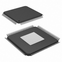
SCAN25100TYA/NOPB National Semiconductor, SCAN25100TYA/NOPB Datasheet - Page 10

SCAN25100TYA/NOPB
Manufacturer Part Number
SCAN25100TYA/NOPB
Description
IC SERIAL/DESERIAL CPRI 100-TQFP
Manufacturer
National Semiconductor
Series
SCANr
Datasheet
1.SCAN25100TYANOPB.pdf
(34 pages)
Specifications of SCAN25100TYA/NOPB
Function
Serializer/Deserializer
Data Rate
2.5Gbps
Input Type
LVTTL/LVCMOS
Output Type
LVTTL, LVCMOS
Number Of Inputs
10
Number Of Outputs
10
Voltage - Supply
1.7 V ~ 1.9 V
Operating Temperature
-40°C ~ 85°C
Mounting Type
Surface Mount
Package / Case
100-TQFP Exposed Pad, 100-eTQFP, 100-HTQFP, 100-VQFP
Operating Temperature (min)
-40C
Operating Temperature Classification
Industrial
Operating Temperature (max)
85C
Package Type
TQFP EP
Rad Hardened
No
Lead Free Status / RoHS Status
Lead free / RoHS Compliant
Other names
SCAN25100TYA
Available stocks
Company
Part Number
Manufacturer
Quantity
Price
Company:
Part Number:
SCAN25100TYA/NOPB
Manufacturer:
NS
Quantity:
158
Company:
Part Number:
SCAN25100TYA/NOPB
Manufacturer:
Texas Instruments
Quantity:
10 000
www.national.com
RECEIVER OUTPUT TIMING SPECIFICATIONS (Read Mode RXCLKMODE=1, 1228.8 and 614.4 Mbps only)
t
t
f
t
RECEIVER OUTPUT TIMING SPECIFICATIONS (Write Mode RXCLKMODE=0)
t
t
t
f
t
CDET OUTPUT TIMING SPECIFICATIONS (Read Mode RXCLKMODE=1, 1228.8 and 614.4 Mbps only)
t
CDET OUTPUT TIMING SPECIFICATIONS (Write Mode RXCLKMODE=0) (Note 5)
t
t
SYSCLK LVDS OUTPUT TIMING SPECIFICATIONS
t
JIT
t
MDC/MDIO TIMING SPECIFICATIONS (Clause 45)
f
t
t
t
t
MINIMUM PULSE WIDTH, Hardware Reset (Note 13)
t
t
t
PDRX
DC
RXCLKR
R
S-R
H-R
DC
RXCLK
R
PDCD
S-C
H-C
SYSCLKNDC
R
MDC
S-MDIO
H-MDIO
D-MDIO
X-MDIO
TX-RST
RX-RST
RST
, t
, t
, t
Symbol
SYSCLK
F
F
F
RXCLK Propagation Delay
Duty cycle
RXCLK input frequency
Output data transition time
Setup Time
Hold Time
Duty cycle
RXCLK frequency
Output data transition time
CDET Propagation Delay
Setup Time
Hold Time
Duty cycle
Cycle to cycle jitter
Output transition time
MDC Frequency
Setup Time
Hold Time
Delay Time
Transition Time
Transmiter Reset
Receiver Reset
SerDes Reset
Parameter
RXCLK rising or falling edge to
ROUT [9:0] valid
RXCLK input duty cycle
RXCLK input frequency
For ROUT [0-9], LOCK, etc. pins.
Measured between 20% and 80%
levels
ROUT [9:0] valid to RXCLK rising or
falling edge (Note 11)
RXCLK rising or falling edge to
ROUT [9:0] valid (Note 11)
RXCLK duty cycle
For ROUT [0-9], LOCK, etc. pins.
Measured between 20% and 80%
levels
RXCLK rising or falling edge to
CDET
CDET valid to RXCLK rising or
falling edge
RXCLK rising or falling edge to
CDET valid
(Note 12)
Between 20% and 80% levels
(Note 12)
MDIO (input) valid to MDC rising
clock
MDC rising edge to MDIO (input)
invalid
MDIO (output) delay from MDC
rising edge
Measured at MDIO when used as
output, CL = 470 pF
TXPWDNB = 0
RXPWDNB = 0
RESETB = 0
Condition
10
Min
0.9
0.9
1.1
0.1
45
30
45
30
40
10
10
2
2
1
0
0
(Note 2)
0.35
0.35
Typ
1.5
1.5
40
4
4
1
1
1
1
Max
62.5
125
300
0.3
2.5
55
55
60
65
6
6
ps p-p
Units
MHz
MHz
MHz
ns
ns
ns
ns
ns
ns
ns
ns
ns
ns
ns
ns
ns
us
us
us
%
%
%


